
M0170 40-pin Molex Straight Flex Cable, 70mm
70 mm one-to-one extension flex for the 40-pin Molex SSB RP connector, passing every signal to an M0178 ToF or other 40-pin sensor.
Table of contents
Overview
The M0170 is a 70 mm straight extension flex for the ModalAI 40-pin Molex SSB RP connector format introduced with the M0178 Time of Flight (ToF) module. It connects the 40-pin ToF connector on an M0173 Starling 2 front end or an M0172 ToF + hi-res adapter to the M0178, and is the drop-in replacement for the shorter M0177 Starling 2 ToF flex when that cable cannot reach.
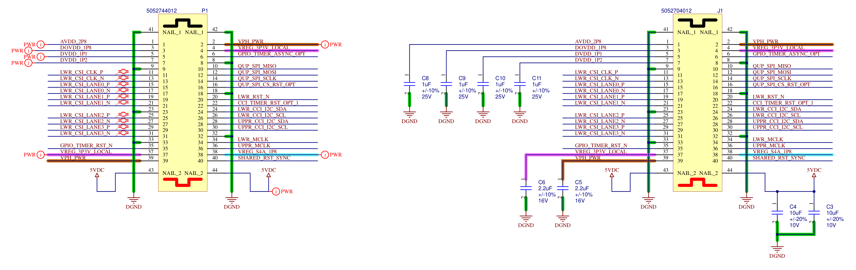
Unlike the M0177, which routes only the ToF signals, the M0170 passes all 40 signal positions and both power nail pairs one to one. It therefore also carries the four-lane CSI group, the upper camera group’s I2C and MCLK, the SPI and timer sideband signals, and the additional sensor supply rails defined for the 40-pin format, so it works as a general extension for any future 40-pin sensor adapter. The sensor-side receptacle carries local bypass capacitors on each supply rail so the extra cable length does not degrade the power delivered to the module.
Connection chain:
VOXL 2 <-> M0173 (J3) or M0172 (J1L) <-> M0170 <-> M0178 <-> IRS2975C ToF sensor
Use the M0170 in place of the M0177, not in addition to it. Chaining flexes adds connector mating cycles, risks misalignment, and pushes the MIPI link past what ModalAI has validated. See extending image sensor cable lengths.
Specification
| Specification | Value |
|---|---|
| Part Number | MSU-M0170-1 |
| Function | 40-pin to 40-pin straight extension flex (pin 1 to pin 1), all positions routed |
| Connector Family | Molex Slimstack SSB RP, 40 signal positions plus 4 power nails, 0.35 mm pitch |
| VOXL 2 Side, P1 | Molex 5052744012 plug. Mates with the 40-pin receptacle on M0173 (J3) or M0172 (J1L) |
| Sensor Side, J1 | Molex 5052704012 receptacle, 0.8 mm mate height. Accepts the M0178 or M0171 P1 plug |
| Length | 70 mm |
| Power Rating | 3 A on the power nail pair (Molex SSB RP power contacts) |
| Bypass Capacitors (J1) | 2 x 10 uF on 5 V; 2.2 uF on 3.3 V; 2.2 uF on VPH_PWR; 1 uF each on AVDD_2P8, DOVDD_1P8, DVDD_1P1, DVDD_1P2 |
| PCB | Polyimide flex, 3 layers, 100 ohm differential impedance control on the CSI pairs |
| Schematic Revision | SCH-M0170 Rev B, March 2024. Rev C (May 2025) is the same design migrated to Altium with no electrical changes |
Pinout
The flex is straight through: pin N on P1 connects to pin N on J1. The net names below follow the 40-pin connector definition used on the host adapters; only the subset listed on the M0178 datasheet is used by that module, and the remaining positions are reserved for other 40-pin sensor adapters.
| Pin # | Signal | Notes | Pin # | Signal | Notes |
|---|---|---|---|---|---|
| 41 | GND (NAIL_1) | Power nail, ground | 42 | GND (NAIL_1) | Power nail, ground |
| 1 | AVDD_2P8 | 2.8 V analog sensor supply, 1 uF bypass at J1 | 2 | VPH_PWR | 3.8 V primary power, 2.2 uF bypass at J1 |
| 3 | DOVDD_1P8 | 1.8 V I/O supply, 1 uF bypass at J1 | 4 | VREG_3P3V_LOCAL | 3.3 V, 2.2 uF bypass at J1 |
| 5 | DVDD_1P1 | 1.1 V digital core supply, 1 uF bypass at J1 | 6 | GPIO_TIMER_ASYNC_OPT | Optional timer / async GPIO |
| 7 | DVDD_1P2 | 1.2 V digital core supply, 1 uF bypass at J1 | 8 | GND | |
| 9 | GND | 10 | QUP_SPI_MISO | Optional SPI | |
| 11 | LWR_CSI_CLK_P | MIPI CSI clock, lower camera group | 12 | QUP_SPI_MOSI | Optional SPI |
| 13 | LWR_CSI_CLK_N | MIPI CSI clock, lower camera group | 14 | QUP_SPI_SCLK | Optional SPI |
| 15 | LWR_CSI_LANE0_P | MIPI CSI data lane 0 | 16 | QUP_SPI_CS_RST_OPT | Optional SPI chip select / reset (CCI_TIMER_RST_OPT_0 on Rev B) |
| 17 | LWR_CSI_LANE0_N | MIPI CSI data lane 0 | 18 | GND | |
| 19 | LWR_CSI_LANE1_P | MIPI CSI data lane 1 | 20 | LWR_RST_N | Sensor reset, lower camera group |
| 21 | LWR_CSI_LANE1_N | MIPI CSI data lane 1 | 22 | CCI_TIMER_RST_OPT_1 | Optional CCI timer / reset |
| 23 | GND | 24 | LWR_CCI_I2C_SDA | CCI I2C data, lower camera group, 1.8 V | |
| 25 | LWR_CSI_LANE2_P | MIPI CSI data lane 2 | 26 | LWR_CCI_I2C_SCL | CCI I2C clock, lower camera group, 1.8 V |
| 27 | LWR_CSI_LANE2_N | MIPI CSI data lane 2 | 28 | UPPR_CCI_I2C_SDA | CCI I2C data, upper camera group |
| 29 | LWR_CSI_LANE3_P | MIPI CSI data lane 3 | 30 | UPPR_CCI_I2C_SCL | CCI I2C clock, upper camera group |
| 31 | LWR_CSI_LANE3_N | MIPI CSI data lane 3 | 32 | GND | |
| 33 | GND | 34 | LWR_MCLK | Sensor master clock, lower camera group, 1.8 V | |
| 35 | GPIO_TIMER_RST_N | Optional timer reset GPIO | 36 | UPPR_MCLK | Sensor master clock, upper camera group |
| 37 | VREG_3P3V_LOCAL | 3.3 V | 38 | VREG_S4A_1P8 | 1.8 V VDDIO (VREG_S4A) |
| 39 | VPH_PWR | 3.8 V primary power | 40 | SHARED_RST_SYNC | Shared reset / sync |
| 43 | 5VDC (NAIL_2) | Power nail, 5 V, 2 x 10 uF bypass at J1 | 44 | 5VDC (NAIL_2) | Power nail, 5 V |
The power nails are numbered 41 through 44 and sit at both ends of the connector, with 41 and 42 nearest pin 1. When mating, confirm pin 1 lines up with pin 1 on both ends. The M0178 datasheet has a labeled connector drawing.
Schematic
Compatibility
| Item | Value |
|---|---|
| VOXL 2 adapters | M0173 J3 (Starling 2 front end), M0172 J1L (ToF + hi-res adapter) |
| ToF modules | M0178 (Starling 2 ToF adapter with mounting tab), M0171 (same without the tab) |
| Sensor type in voxl-camera-server | pmd-tof-liow2 |
| Shorter alternative | M0177, the Starling 2 ToF flex shipped in the kit |