
M0195 VOXL 2 Mini Stinger Imager Adapter
Stinger imager adapter breaking out VOXL 2 Mini camera groups J6 and J7.
Table of contents
- Summary
- Hardware
- Software
Summary
Features
M0195 Serves as a breakout for Camera Groups J6 and J7 on VOXL 2 Mini.
- Micro Coax camera connections
- 2 one lane MIPI-CSI in combo mode for CV (AR0144, M0166)
- 2 four lane MIPI-CSI for EO (IMX664, M0161)
- 1 two lane MIPI-CSI for Thermal (Boson+)
- image sensor hardware synchronization
- 2 FLIR Lepton 3.5 sensor interfaces (1 natively, another using an additional cable to route to an extra SPI)
- 2 channel I2C mux (TCA9543A, address 0x73)
- 1 I2C connection for ModalAI VTX power monitoring (on /dev/i2c-0, ADC address 0x1D, Temp address 0x48)
- 1 ICP-10100 Barometer (on /dev/i2c-0, address 0x63)
Hardware Requirements
- Only compatible with VOXL 2 Mini
- Micro-coax Cables MCBL-00084
VOXL SDK Requirements
VOXL SDK 1.5.0+ is required.
Kernel Requirements for M0195
M0195 requires kernel m0104-1-var00.2-kernel.img.
When installing SDK, select “D0013” option to install this kernel.
Dimensions
3D Drawings
TODO
2D Drawings
TODO
Specifications
| Feature | Details |
|---|---|
| Weight | TODO g |
| HxW | TODO |
Hardware
Connectors
Summary
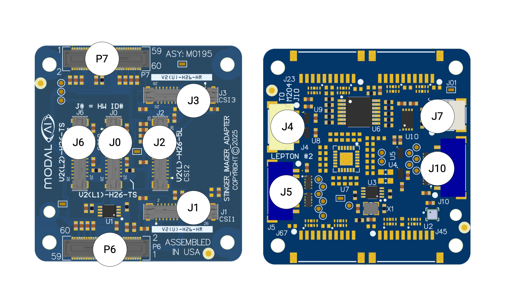
Hover a connector to identify it — click to jump to its pinout.
| Connector | Description |
|---|---|
| J0 | Tracking Sensor ID0 |
| J1 | Hires Sensor ID1 |
| J2 | Thermal Sensor ID2 |
| J3 | Hires Sensor ID3 |
| J6 | Tracking Sensor ID6 |
| Connector | Description |
|---|---|
| P6 | Board to Board - mates to M0204 J6 |
| P7 | Board to Board - mates to M0204 J7 |
| Connector | Description |
|---|---|
| J4 | Connects to M0204 J10 SPI (For Lepton 2) |
| J5 | FLIR Leptopn 2 |
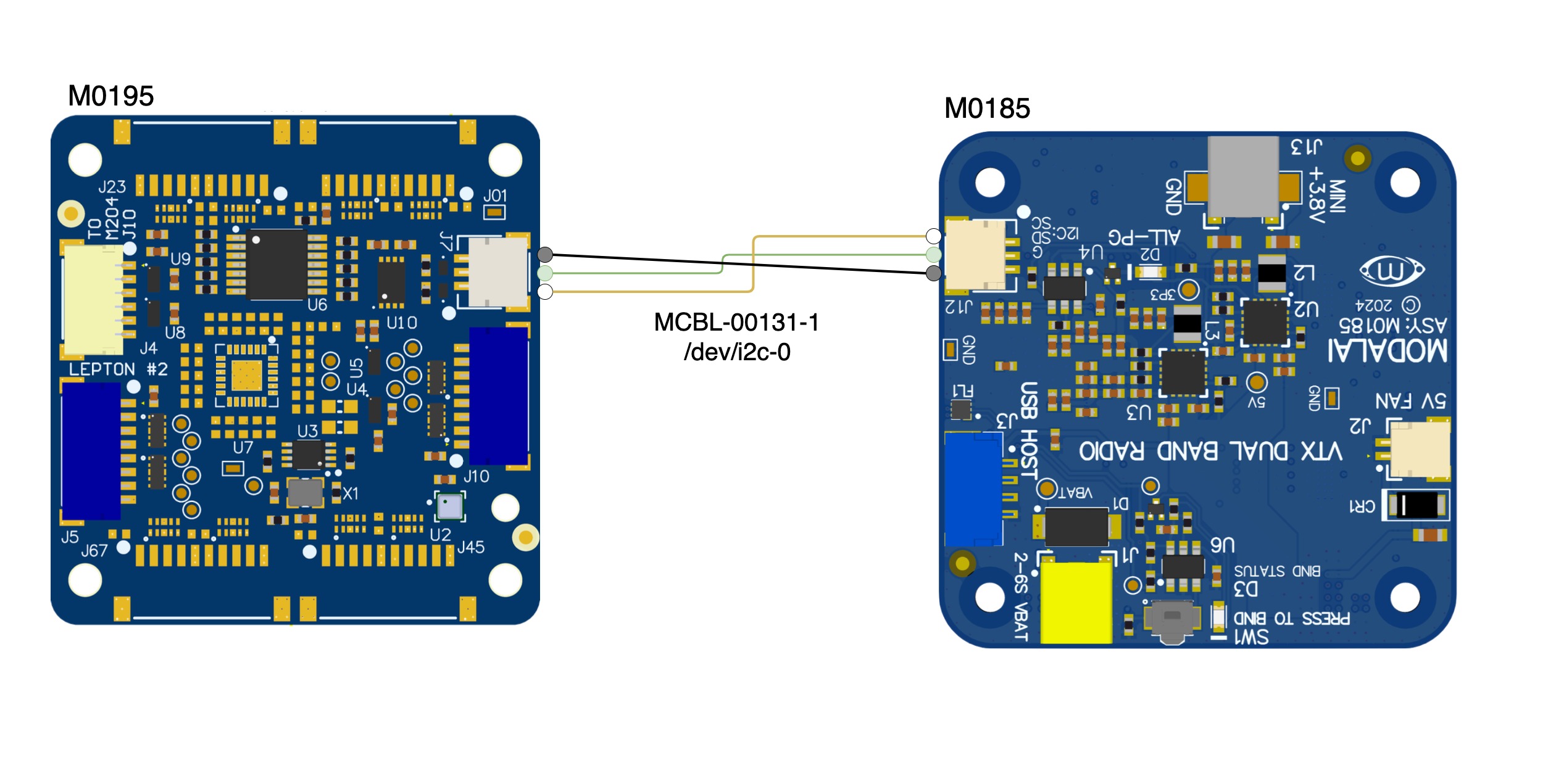
| J7 | ModalAI VTX power monitoring I2C |
| J10 | FLIR Leptopn 1 |
Board-to-Board Connectors
P6 and P7 are Hirose DF40HC(4.0)-60DS-0.4V(51) 60-pin connectors with a 4 mm mate height. They mate with the VOXL 2 Mini camera group connectors J6 and J7.
P6 - Camera Group 0 (mates to VOXL 2 Mini J6)
P6 carries CSI0 (J0 and J6 tracking sensors) and CSI1 (J1 hires sensor), plus the CAM0 SPI0 port used by Lepton 1.
| Pin # | Signal | Pin # | Signal |
|---|---|---|---|
| 1 | DGND | 2 | DGND |
| 3 | CCI_I2C0_SDA | 4 | PM8009_VREG_L2_DVDD_1P2 |
| 5 | CCI_I2C0_SCL | 6 | PM8009_VREG_L7_DOVDD_1P8 |
| 7 | DGND | 8 | PM8009_VREG_L1_DVDD_1P05 |
| 9 | CSI0_CLK_CON_P | 10 | GPIO_93_CAM0_RST_N |
| 11 | CSI0_CLK_CON_N | 12 | GPIO_94_MCLK0 |
| 13 | CSI0_LANE0_CON_P | 14 | DGND |
| 15 | CSI0_LANE0_CON_N | 16 | GPIO_110_CCI_TIMER1 |
| 17 | DGND | 18 | GPIO_113_CCI_TIMER4 |
| 19 | CSI0_LANE1_CON_P | 20 | GPIO_95_MCLK1 |
| 21 | CSI0_LANE1_CON_N | 22 | PM8009_VREG_L5_AVDD_2P8 |
| 23 | CSI0_LANE2_CON_P | 24 | DGND |
| 25 | CSI0_LANE2_CON_N | 26 | GPIO_109_GSYNC |
| 27 | DGND | 28 | CCI_I2C1_SDA |
| 29 | CSI0_LANE3_CON_P | 30 | CCI_I2C1_SCL |
| 31 | CSI0_LANE3_CON_N | 32 | Not connected |
| 33 | DGND | 34 | GPIO_28_CAM0_SPI0_MISO |
| 35 | CSI1_CLK_CON_P | 36 | Not connected |
| 37 | CSI1_CLK_CON_N | 38 | GPIO_30_CAM0_SPI0_CLK |
| 39 | CSI1_LANE0_CON_P | 40 | GPIO_31_CAM0_SPI0_CS |
| 41 | CSI1_LANE0_CON_N | 42 | VREG_S4A_1P8 |
| 43 | DGND | 44 | DGND |
| 45 | CSI1_LANE1_CON_P | 46 | VPH_PWR |
| 47 | CSI1_LANE1_CON_N | 48 | VPH_PWR |
| 49 | CSI1_LANE2_CON_P | 50 | DGND |
| 51 | CSI1_LANE2_CON_N | 52 | VREG_3P3V_LOCAL |
| 53 | DGND | 54 | DGND |
| 55 | CSI1_LANE3_CON_P | 56 | VDC_5V_LOCAL |
| 57 | CSI1_LANE3_CON_N | 58 | VDC_5V_LOCAL |
| 59 | DGND | 60 | DGND |
P7 - Camera Group 1 (mates to VOXL 2 Mini J7)
P7 carries CSI2 (J2 thermal sensor, two lanes) and CSI3 (J3 hires sensor). GPIO_4 and GPIO_5 (QUP1) run in I2C mode and serve the barometer, the TCA9543A Lepton I2C mux, the VTX I2C on J7, and J2.
| Pin # | Signal | Pin # | Signal |
|---|---|---|---|
| 1 | DGND | 2 | DGND |
| 3 | CCI_I2C2_SDA | 4 | PM8009_VREG_L2_DVDD_1P2 |
| 5 | CCI_I2C2_SCL | 6 | PM8009_VREG_L7_DOVDD_1P8 |
| 7 | DGND | 8 | PM8009_VREG_L1_DVDD_1P05 |
| 9 | CSI2_CLK_CON_P | 10 | GPIO_92_CAM1_RST_N |
| 11 | CSI2_CLK_CON_N | 12 | GPIO_96_MCLK2 (test point only) |
| 13 | CSI2_LANE0_CON_P | 14 | DGND |
| 15 | CSI2_LANE0_CON_N | 16 | GPIO_111_CCI_TIMER2 (test point only) |
| 17 | DGND | 18 | GPIO_114_CCI_ASYNC_IN |
| 19 | CSI2_LANE1_CON_P | 20 | GPIO_97_MCLK3 |
| 21 | CSI2_LANE1_CON_N | 22 | PM8009_VREG_L6_AVDD_2P8 |
| 23 | Not connected | 24 | DGND |
| 25 | Not connected | 26 | GPIO_109_GSYNC |
| 27 | DGND | 28 | CCI_I2C3_SDA |
| 29 | Not connected | 30 | CCI_I2C3_SCL |
| 31 | Not connected | 32 | GPIO_100_CAM_SHARED_RST_N (test point only) |
| 33 | DGND | 34 | GPIO_4_CAM1_SPI1_MISO |
| 35 | CSI3_CLK_CON_P | 36 | GPIO_5_CAM1_SPI1_MOSI |
| 37 | CSI3_CLK_CON_N | 38 | GPIO_6_CAM1_SPI1_CLK |
| 39 | CSI3_LANE0_CON_P | 40 | GPIO_7_CAM1_SPI1_CS |
| 41 | CSI3_LANE0_CON_N | 42 | VREG_S4A_1P8 |
| 43 | DGND | 44 | DGND |
| 45 | CSI3_LANE1_CON_P | 46 | VPH_PWR |
| 47 | CSI3_LANE1_CON_N | 48 | VPH_PWR |
| 49 | CSI3_LANE2_CON_P | 50 | DGND |
| 51 | CSI3_LANE2_CON_N | 52 | VREG_3P3V_LOCAL |
| 53 | DGND | 54 | DGND |
| 55 | CSI3_LANE3_CON_P | 56 | VDC_5V_LOCAL |
| 57 | CSI3_LANE3_CON_N | 58 | VDC_5V_LOCAL |
| 59 | DGND | 60 | DGND |
Image Sensor Interfaces
- requires kernel
m0104-1-var00.2-kernel.img
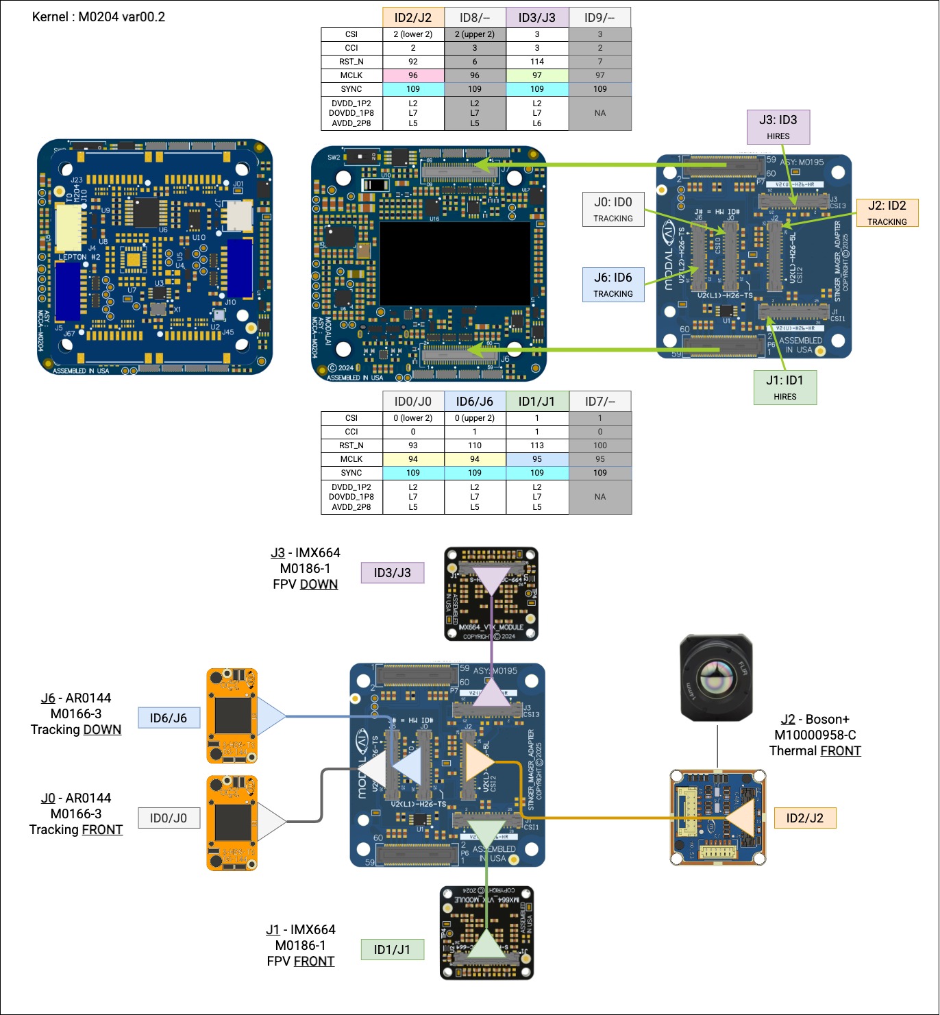
MIPI Connection Details
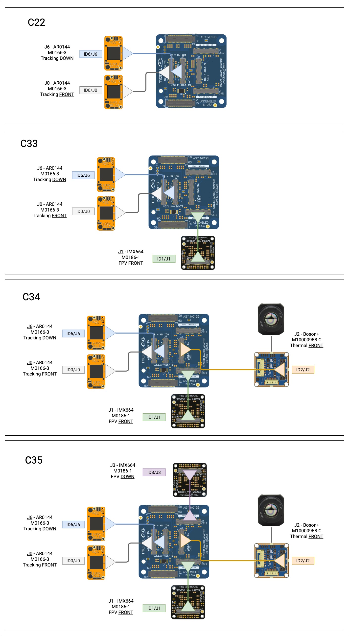
Support Camera Configs
Notes for Sensors
- supported coax cables
- HW synchronization
- tracking sensors enabled sync by default using GPIO 109 (voxl-fsync-mod)
- hires sensors are not synced by default: their sync pins (J1 and J3 pin 21) connect to GPIO 109 only through R10 and R11, which are not fitted
- the Boson+ on J2 receives GPIO 109 directly on pin 17
- connectors
- J0, J1, J2, J3, and J6 are Hirose DF56C-26S-0.3V(51) 26-pin micro-coax receptacles
J0 - Tracking Sensor ID0
- supported image sensors
- M0166 - 1280x800 Global Shutter Sensor AR0144
- 2 MIPI lane support, in combo mode with Sensor ID6
| Pin # | Signal | Notes |
|---|---|---|
| 1 | CCI_I2C0_SDA | CCI I2C |
| 2 | PM8009_VREG_L2_DVDD_1P2 | 1.2 V digital core supply |
| 3 | CCI_I2C0_SCL | CCI I2C |
| 4 | PM8009_VREG_L2_DVDD_1P2 | 1.2 V digital core supply |
| 5 | DGND | |
| 6 | DGND | |
| 7 | CSI0_CLK_CON_P | |
| 8 | PM8009_VREG_L2_DVDD_1P2 | 1.2 V digital core supply |
| 9 | CSI0_CLK_CON_N | |
| 10 | PM8009_VREG_L7_DOVDD_1P8 | 1.8 V I/O supply |
| 11 | CSI0_LANE0_CON_P | |
| 12 | GPIO_93_CAM0_RST_N | Reset |
| 13 | CSI0_LANE0_CON_N | |
| 14 | CSI0_LANE1_CON_P | |
| 15 | MCLK0_ID0 | MCLK, buffered from GPIO_94_MCLK0 |
| 16 | CSI0_LANE1_CON_N | |
| 17 | DGND | |
| 18 | DGND | |
| 19 | PM8009_VREG_L5_AVDD_2P8 | 2.8 V analog supply |
| 20 | Not connected | |
| 21 | TRACK_TRIG_ID0 | Frame sync, GPIO_109_GSYNC through R5/R6 |
| 22 | Not connected | |
| 23 | DGND | |
| 24 | Not connected | |
| 25 | VPH_PWR | Not used by AR0144 |
| 26 | Not connected | |
| S1-S5 | DGND | Shield |
J1 - Hires Sensor ID1
- supported image sensors
- M0161 - 4k High-resolution, Low-light, IMX412
- 4 MIPI lane support
| Pin # | Signal | Notes |
|---|---|---|
| 1 | CCI_I2C1_SDA | CCI I2C |
| 2 | PM8009_VREG_L2_DVDD_1P2 | 1.2 V digital core supply |
| 3 | CCI_I2C1_SCL | CCI I2C |
| 4 | PM8009_VREG_L2_DVDD_1P2 | 1.2 V digital core supply |
| 5 | DGND | |
| 6 | DGND | |
| 7 | CSI1_CLK_CON_P | |
| 8 | PM8009_VREG_L2_DVDD_1P2 | 1.2 V digital core supply |
| 9 | CSI1_CLK_CON_N | |
| 10 | PM8009_VREG_L7_DOVDD_1P8 | 1.8 V I/O supply |
| 11 | CSI1_LANE0_CON_P | |
| 12 | GPIO_113_CCI_TIMER4 | Reset |
| 13 | CSI1_LANE0_CON_N | |
| 14 | CSI1_LANE1_CON_P | |
| 15 | GPIO_95_MCLK1 | MCLK |
| 16 | CSI1_LANE1_CON_N | |
| 17 | DGND | |
| 18 | DGND | |
| 19 | PM8009_VREG_L5_AVDD_2P8 | 2.8 V analog supply |
| 20 | CSI1_LANE2_CON_P | |
| 21 | HIRES_SYNC_ID1 | Not connected by default (R10 not fitted) |
| 22 | CSI1_LANE2_CON_N | |
| 23 | DGND | |
| 24 | CSI1_LANE3_CON_P | |
| 25 | VPH_PWR | |
| 26 | CSI1_LANE3_CON_N | |
| S1-S5 | DGND | Shield |
J2 - Thermal Sensor ID2
- supported image sensors
- Boson+ (M0201 backpack)
- 2 MIPI lane support
| Pin # | Signal | Notes |
|---|---|---|
| 1 | DGND | |
| 2 | GPIO_92_CAM1_RST_N | Reset |
| 3 | CSI2_CLK_CON_P | |
| 4 | GPIO_6_CAM1_SPI1_CLK | QUP1 lane 2 |
| 5 | CSI2_CLK_CON_N | |
| 6 | DGND | |
| 7 | DGND | |
| 8 | DGND | |
| 9 | CSI2_LANE0_CON_P | |
| 10 | VREG_S4A_1P8 | 1.8 V |
| 11 | CSI2_LANE0_CON_N | |
| 12 | GPIO_7_CAM1_SPI1_CS | QUP1 lane 3 |
| 13 | DGND | |
| 14 | CSI2_LANE1_CON_P | |
| 15 | DGND | |
| 16 | CSI2_LANE1_CON_N | |
| 17 | GPIO_109_GSYNC | Frame sync |
| 18 | DGND | |
| 19 | VDC_5V_LOCAL | 5 V |
| 20 | CCI_I2C2_SDA | CCI I2C |
| 21 | VDC_5V_LOCAL | 5 V |
| 22 | CCI_I2C2_SCL | CCI I2C |
| 23 | VDC_5V_LOCAL | 5 V |
| 24 | GPIO_4_CAM1_SPI1_MISO | QUP1 I2C SDA |
| 25 | VDC_5V_LOCAL | 5 V |
| 26 | GPIO_5_CAM1_SPI1_MOSI | QUP1 I2C SCL |
| S1-S5 | DGND | Shield |
J3 - Hires Sensor ID3
- supported image sensors
- M0161 - 4k High-resolution, Low-light, IMX412
- 4 MIPI lane support
| Pin # | Signal | Notes |
|---|---|---|
| 1 | CCI_I2C3_SDA | CCI I2C |
| 2 | PM8009_VREG_L2_DVDD_1P2 | 1.2 V digital core supply |
| 3 | CCI_I2C3_SCL | CCI I2C |
| 4 | PM8009_VREG_L2_DVDD_1P2 | 1.2 V digital core supply |
| 5 | DGND | |
| 6 | DGND | |
| 7 | CSI3_CLK_CON_P | |
| 8 | PM8009_VREG_L2_DVDD_1P2 | 1.2 V digital core supply |
| 9 | CSI3_CLK_CON_N | |
| 10 | PM8009_VREG_L7_DOVDD_1P8 | 1.8 V I/O supply |
| 11 | CSI3_LANE0_CON_P | |
| 12 | GPIO_114_CCI_ASYNC_IN | Reset |
| 13 | CSI3_LANE0_CON_N | |
| 14 | CSI3_LANE1_CON_P | |
| 15 | GPIO_97_MCLK3 | MCLK |
| 16 | CSI3_LANE1_CON_N | |
| 17 | DGND | |
| 18 | DGND | |
| 19 | PM8009_VREG_L6_AVDD_2P8 | 2.8 V analog supply |
| 20 | CSI3_LANE2_CON_P | |
| 21 | HIRES_SYNC_ID3 | Not connected by default (R11 not fitted) |
| 22 | CSI3_LANE2_CON_N | |
| 23 | DGND | |
| 24 | CSI3_LANE3_CON_P | |
| 25 | VPH_PWR | |
| 26 | CSI3_LANE3_CON_N | |
| S1-S5 | DGND | Shield |
J6 - Tracking Sensor ID6
- supported image sensors
- M0166 - 1280x800 Global Shutter Sensor AR0144
- 2 MIPI lane support, in combo mode with Sensor ID0
| Pin # | Signal | Notes |
|---|---|---|
| 1 | CCI_I2C1_SDA | CCI I2C |
| 2 | PM8009_VREG_L2_DVDD_1P2 | 1.2 V digital core supply |
| 3 | CCI_I2C1_SCL | CCI I2C |
| 4 | PM8009_VREG_L2_DVDD_1P2 | 1.2 V digital core supply |
| 5 | DGND | |
| 6 | DGND | |
| 7 | CSI0_LANE3_CON_P | Clock in combo mode |
| 8 | PM8009_VREG_L2_DVDD_1P2 | 1.2 V digital core supply |
| 9 | CSI0_LANE3_CON_N | Clock in combo mode |
| 10 | PM8009_VREG_L7_DOVDD_1P8 | 1.8 V I/O supply |
| 11 | CSI0_LANE2_CON_P | Data lane 0 in combo mode |
| 12 | GPIO_110_CCI_TIMER1 | Reset |
| 13 | CSI0_LANE2_CON_N | Data lane 0 in combo mode |
| 14 | Not connected | |
| 15 | MCLK0_ID6 | MCLK, buffered from GPIO_94_MCLK0 |
| 16 | Not connected | |
| 17 | DGND | |
| 18 | DGND | |
| 19 | PM8009_VREG_L5_AVDD_2P8 | 2.8 V analog supply |
| 20 | Not connected | |
| 21 | TRACK_TRIG_ID6 | Frame sync, GPIO_109_GSYNC through R5/R7 |
| 22 | Not connected | |
| 23 | DGND | |
| 24 | Not connected | |
| 25 | VPH_PWR | Not used by AR0144 |
| 26 | Not connected | |
| S1-S5 | DGND | Shield |
FLIR Lepton Interfaces
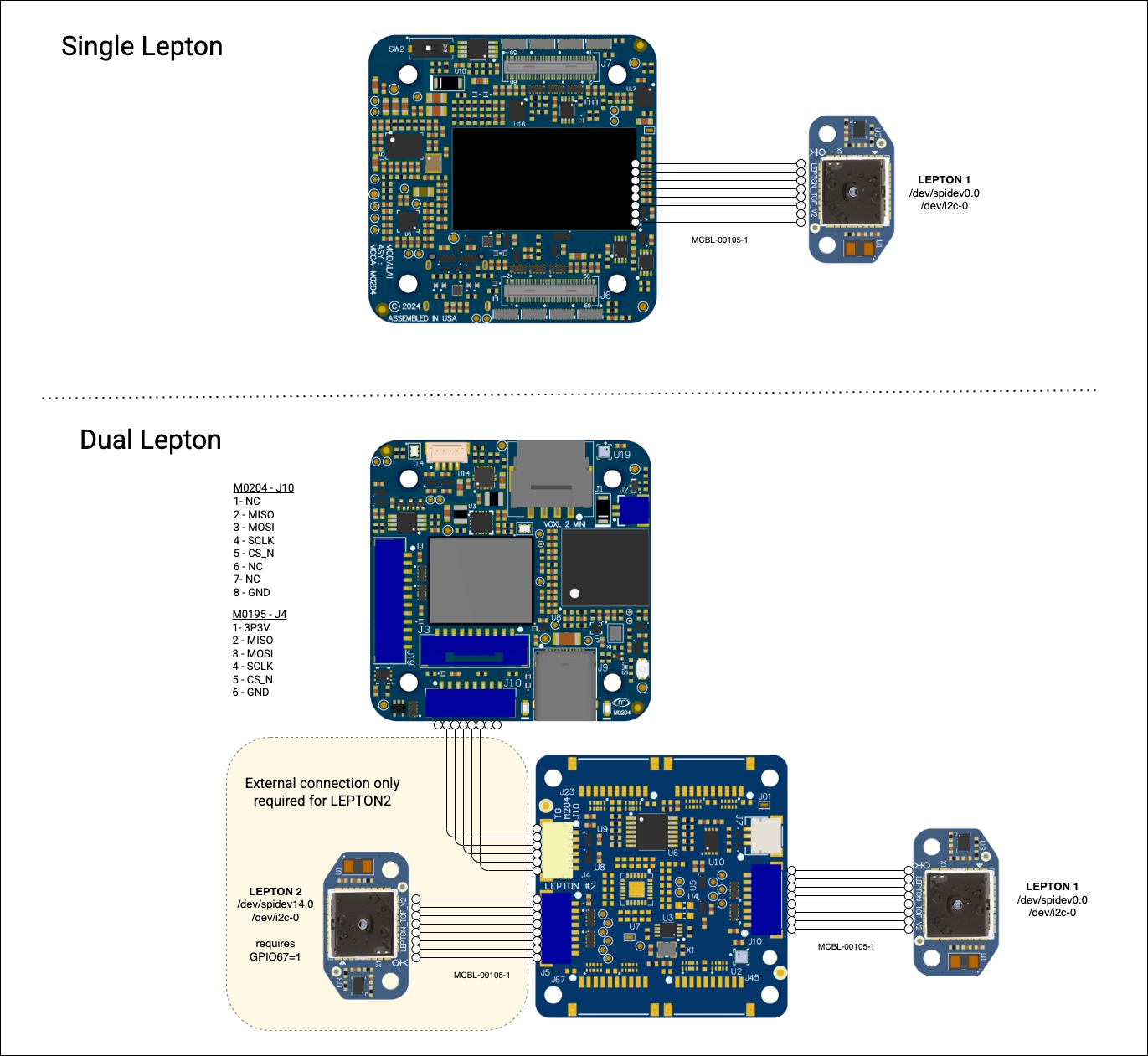
Lepton 1 - J10
J10 and J5 are JST SM08B-SRSS-TB 8-pin 1.0 mm connectors with the same pinout. The SPI, I2C, and clock lines run at 2.8 V, and the board’s level translators and 25 MHz oscillator handle the conversion.
| Pin # | Signal | Notes |
|---|---|---|
| 1 | VREG_AVDD_2P8_FLIR | 2.8 V, from PM8009_VREG_L5_AVDD_2P8 |
| 2 | FLIR1_SPI_SCK_2P8V | CAM0 SPI0, level-shifted from 1.8 V |
| 3 | FLIR1_SPI_CS_N_2P8V | CAM0 SPI0, level-shifted from 1.8 V |
| 4 | FLIR1_SPI_MISO_2P8V | CAM0 SPI0, level-shifted from 1.8 V |
| 5 | FLIR1_I2C_SCL_2P8V | TCA9543A channel 0 |
| 6 | FLIR1_I2C_SDA_2P8V | TCA9543A channel 0 |
| 7 | CLK_25M_FLIR1_2P8V | 25 MHz reference clock |
| 8 | DGND | |
| S1, S2 | DGND |
Lepton 2 - J5 (external SPI to M0104 J10)
Lepton 2’s SPI comes from VOXL 2 Mini J10 through J4, not from the camera group connectors.
| Pin # | Signal | Notes |
|---|---|---|
| 1 | VREG_AVDD_2P8_FLIR | 2.8 V, from PM8009_VREG_L5_AVDD_2P8 |
| 2 | FLIR2_SPI_SCK_2P8V | From J4, level-shifted from 3.3 V |
| 3 | FLIR2_SPI_CS_N_2P8V | From J4, level-shifted from 3.3 V |
| 4 | FLIR2_SPI_MISO_2P8V | From J4, level-shifted from 3.3 V |
| 5 | FLIR2_I2C_SCL_2P8V | TCA9543A channel 1 |
| 6 | FLIR2_I2C_SDA_2P8V | TCA9543A channel 1 |
| 7 | CLK_25M_FLIR2_2P8V | 25 MHz reference clock |
| 8 | DGND | |
| S1, S2 | DGND |
J4 - SPI from VOXL 2 Mini J10
J4 is a JST SM06B-SRSS-TB 6-pin 1.0 mm connector. It takes the 3.3 V SPI port from VOXL 2 Mini J10 and passes it to Lepton 2 on J5. The MCBL-00120-1 cable converts J10’s 8-pin GH connector to this 6-pin SH connector.
| Pin # | Signal | Notes |
|---|---|---|
| 1 | VREG_3P3V_LOCAL | 3.3 V |
| 2 | V2MINIJ10_SPI_MISO_3P3V | |
| 3 | V2MINIJ10_SPI_MOSI_3P3V | Not used on M0195 |
| 4 | V2MINIJ10_SPI_SCLK_3P3V | |
| 5 | V2MINIJ10_SPI_CS0_3P3V | |
| 6 | DGND | |
| S1, S2 | DGND |
ModalAI VTX I2C Interface
dev/i2c-0 - ADC address 0x1D, Temp Sensor address 0x48
J7 is a JST SM03B-SRSS-TB 3-pin 1.0 mm connector.
| Pin # | Signal | Notes |
|---|---|---|
| 1 | SENSOR_SCL_3P3V | QUP1 I2C, translated to 3.3 V by PCA9517A |
| 2 | SENSOR_SDA_3P3V | QUP1 I2C, translated to 3.3 V by PCA9517A |
| 3 | DGND | |
| S1, S2 | DGND |
Software
Linux Users Guide
Lepton 1 - J10
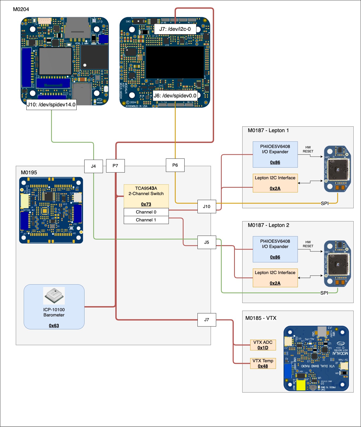
The /dev/spidev0.0 SPI interface comes through M0195 P6, the /dev/i2c-0 I2C inteface comes though M0195 P7.
I2C is shared between Lepton 1 and Lepton 2 and we need to use a channel selector.
For Lepton 1 I2C, you need to use CHANNEL0 of the TCA9543A device (write 0x01 to address 0x01 on slave device 0x73).
Lepton 2 - J5 (external SPI to M0204 J10)
The /dev/spidev14.0 SPI interface comes through J4 that connects to M0104 J10 externally, the /dev/i2c-0 I2C inteface comes though P7.
I2C is shared between Lepton 1 and Lepton 2 and we need to use a channel selector.
For I2C, you can use CHANNEL1 of the TCA9543A device (write 0x02 to address 0x01 on slave device 0x73).
Baromter Interface
A ICP-10100 barometer is exposed on /dev/i2c-0 (address 0x63) when M0195 attached to M0204 (VOXL2 Mini)
I2C Mux Interfaces
A 2 channel I2C mux (TCA9543A) is on the /dev/i2c-0 bus at address 0x73 when mated to VOXL2 Mini.