VOXL 2 Developer Test Board User Guide
Table of contents
Overview
The VOXL 2 Developer Test Board (M0144) is the first of-its-kind plug-in expansion board that allows Hardware and Software developers of the VOXL 2 ecosystem to access and utilize all GPIO/QUP signals (and others) from J3 and J5.
Hardware
The VOXL 2 Developer Test Board (M0144) is a companion/test board that accompanies your VOXL 2 boards. It was designed with software and hardware developers in-mind. It was NOT designed with any Mechanical or Flight constraints (purposely large so you do not fly with it!). Prior to this design, there was always a risk that a specific GPIO or QUP port you wanted to use in your end application was not enabled, blocked, or just inaccessible for you to try out first. This created lots of risk both in Software and Hardware development cycles. The “B-Quad” (anecdotally the “Board to Board Breakout Board”) is our way to de-risk that scenario by allowing any hardware or software developer the option to try all potential signal and port mappings on their target hardware before committing to hardware PCB fabrication and/or software releases.
This guide will help you understand how to use this hardware and why it was designed the way it was.
This design has a no RMA policy (non-returnable) due to the excessive handling and opportunities for damage or mis-wiring Exceptions will be made on a case-by-case basis if we agree there is a defect with your particular unit.
Component Arrangement
The design of this board is for direct plug in to VOXL 2 J3 and J5 and allow for mounting hole alignment so that standoffs can be used to secure the boards together at a 5mm mating height.
The High-Speed signals (USB and SD Card) are placed closer to the top so the signal lengths are minimized. We then made sure to place the signal access headers, J14, J15, and J16 with enough room to add clear silkscreen/labeling and allow for fingers to reach in and adjust jumper wires.
All the translated/buffered signals are located at the bottom of the board with right-angle connectors so cables clearly egress away from the board for test equipment needs. The several jumpers on the board ware placed strategically where they are needed. For example, the USB VBUS power selection jumper JP4 is near the USB connector J11. The Connector VTREF selection jumper JP3 is placed down near all of the R/A connectors. Most jumper pins will come with 2-position shorting jumpers on them pre-set as indicated throughout these pages. We intended this design to be easy to view and use without the need for schematics, but of course, we still provide them for your use and understanding.
Reading the Silkscreen
As noticed here, 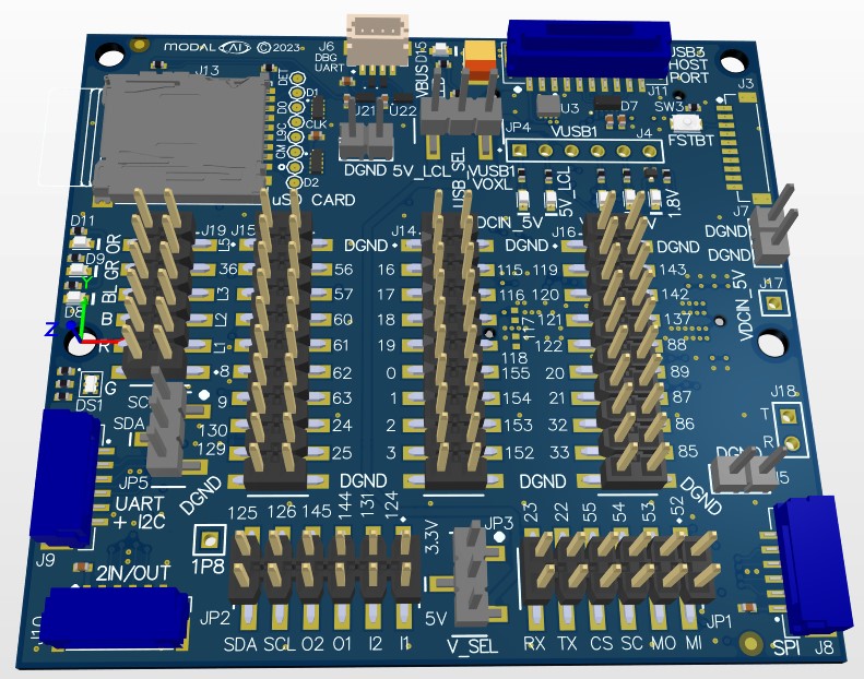 a number or notation is placed next to each header pin in silkscreen, such as in the middle with “DGND, 16, 17, 18, 19, 0, 1, 2, 3, DGND” at J14. Note the pinouts for J14 net names correlate to these GPIO numbers. All pin 1’s for every connector are noted with dots, and the dual row headers always count zig-zag. So, referencing the schematic for J14, notice pin 1 is DGND, pin 3 is GPIO_16_QUP6_L0, pin 5 is GPIO_17_QUP6_L1” and so on.
For another example, refer to JP1 for the SPI port jumper (lower right of image). On the board, note the “RX”, “TX”, “CS”, “SC”, “MO”, and “MI” markings. These correlate with the UART RX, UART TX, SPI_CS_N, SPI_SCLK, SPI_MOSI, and SPI_MISO signals respectively that are directly connected to the 1.8V side of the 1.8V-to-3.3V level translators. Then, using J8 (for SPI) and J9 (for UART), the 3.3V versions of these signals are exposed.
LEDs Switches & Misc
LEDs and switches are all called out here: 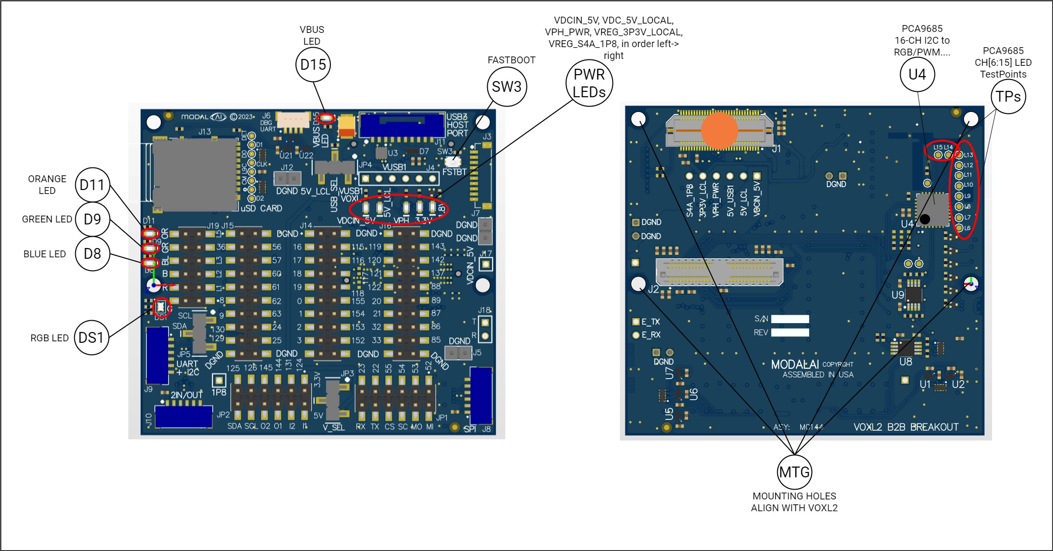
The six power and VBUS LEDs are automatically ON when that respective power rail is active. All GPIO (or PCA9685) controlled LEDs are arranged in order of the connector J19. On the left, notice the labeling “OR”, GR”, “BL”, “B”, “R”, and “G”. The “OR/GR/BL” are the discrete (single) color LEDs, and the “BRG” is for the RGB LED DS1.
This design also exposes a push button for Fastboot that is common across many of our debug boards, as noted above by SW3. Operation of this switch is documented here: https://docs.modalai.com/voxl2-connectors/#sw1—force-fastboot-button
Selecting VBUS using JP4
As shown in the schematic snippet here: 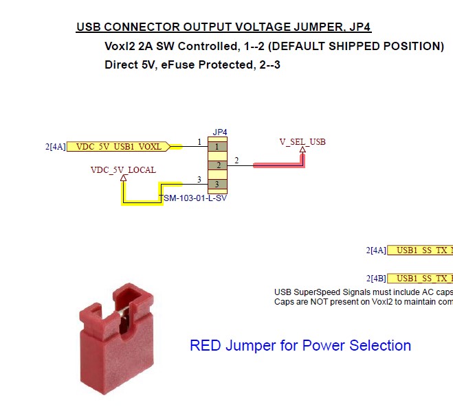 the USB VBUS can be set as either sourced from the 2Amp 5V power rail direct from VOXL 2, J3 pin 16 (controlled by GPIO_157), or it can be sourced by the 5V supply on VOXL 2 VDC_5V_LOCAL. The benefit of one vs the other is up to the user as described here: https://docs.modalai.com/voxl2-dev-test-board-datasheet/#jp4—usb-vbus-j11-selection-jumper To change the setting, make sure the VOXL 2 (and entire system) is powered OFF, then remove the red jumper (provided) from position 1–2 and move it to position 2–3.
Selecting VTREF on J8, J9, and J10 using JP3
As shown in the schematic snippet here:  the pin 1 voltage of J8, J9, and J10 can be set as either 5V or 3.3V. The benefit of one vs the other is up to the user as described here: https://docs.modalai.com/voxl2-dev-test-board-datasheet/#jp3—port-connector-j8-j9-j10-vtref-selection-jumper To change the setting, make sure the VOXL 2 (and entire system) is powered OFF, then remove the red jumper (provided) from position 1–2 and move it to position 2–3. Note the signals on J8-J10 are ALWAYS +3.3V regardless of this jumper selection as observed in the schematic on sheet 5 with each translator device VCCB set as VREG_3P3V_LOCAL.
Selecting an I2C bus for the PCA9685 using JP5
As shown in the schematic snippet here: 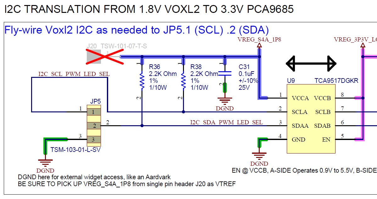 the only way to talk to the PCA9685 device is by connecting some I2C bus to this jumper. If you want a bus that is on one of the signal access headers, such as J15 pins 15 and 17 (I2C10), then simply use one of the flywire jumpers provided with the development kit to connect J15.15 (SCL) to JP5.1, and J15.17 (SDA) to JP5.2 and now the make sure QUP_10 is set up as I2C in software to talk to the PCA9685 device. If you require an external device, such as an Aardvark or other external hardware, then you must also connect a GND connection on JP5.3, and if the devices requires a VTREF to set the signals at 1.8V, use J20 as noted in the schematic. You may install a single pin jumper, or just directly solder a wire into that plated hole.
Selecting specific QUPs for SPI, UART, or I2C on J8-J10
As shown in the schematic snippet here: 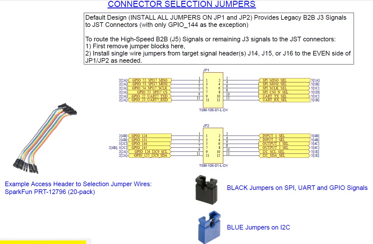 the 6-pin Board to Board connectors are shipped in the default mode as follows:
| Connector | QUP Mapping (Default jumpers) | Set By |
|---|---|---|
| J8, SPI | QUP_17 | JP1: 1–2, 3–4, 5–6, 7–8 |
| J9, UART + I2C | QUP_7 (UART), QUP_9 (I2C) | JP1(UART): 9–10, 11–12 JP2 (I2C)9–10, 11–12 |
| J10 2I/2O | GPIO_124 (IN1), GPIO_131 (IN2), GPIO_144 (OUT1), GPIO_145 (OUT2) | JP2: 1–2, 3–4, 5–6, 7–8 |
To change these settings, make sure the VOXL 2 (and entire system) is powered OFF, then remove the specific JP1/JP2 jumpers you need and flywire in the signals you need from J14-J16 or JP1/JP2 cross-wise.
For example, if you want to change the UART port on J9 from QUP_7 to QUP_11;
- Make sure the VOXL 2 (and entire system) is powered OFF
- Remove JP1 jumpers from 9–10 and 11–12 only
- Locate GPIO_62 and GPIO_63 on J15, pins 12/14 respectively (use the QUP Lane mapping table in the Schematic on Sheet 4 to help you map L0, L1, L2, and L3 to each QUP function as explained in the Hardware User Guide)
- Fly wire from J15.12 (TX) using one of the PRT-12796 jumpers provided to JP1.10.
- Fly wire from J15.14 (RX) using one of the PRT-12796 jumpers provided to JP1.12.
- Power ON your system, and set your software now for QUP_11 in UART mode.
- J9 UART pins (pin 2 and 3) is now set as QUP_11 and at 3.3V CMOS signals!
J8-J10 Cross-QUP Modes
The QUP ports J8-J10 can support limited cross-functional port types. For example, the 2I/2O port can easily support UARTS. Simply map the TX to the OUT pins, and RX to Input pins following similar steps above for changing QUP ports. Vice-versa, the UART port can become a 3rd pair of input and output signals. However, the I2C port is limited to I2C and only slow signals such as GPI/GPO due to the driver types. Edge rates are slowed dramatically due to the I2C translators, and do not expect fast data port functions, such as Fast-UART or SPI on J9.4/J9.5 The SPI port can also be re-mapped as other functions, but note the directions on each pin and be aware that if you push a UART into J8, the RX and TX pins will not map up correctly with all ModalAI connectors. SPI is 3 outputs and only 1 input, as shown in the schematics. By providing the schematics for this design, you are free to use this board as you need and have full access to part numbers of each IC so you can validate use cases we did not plan for. You assume all responsibility for operating it out of the intended modes.
Software
This board is pure hardware and has no micro-controller or other device requiring software programming (Flash memory) on it. All software is executed on VOXL 2. The PCA9685 device is a very common and well-known part for I2C-to-PWM generation and many open-source drivers are available for it. Our Developer guide will get into more details how to use that part. This section will focus more on the hardware configuration.