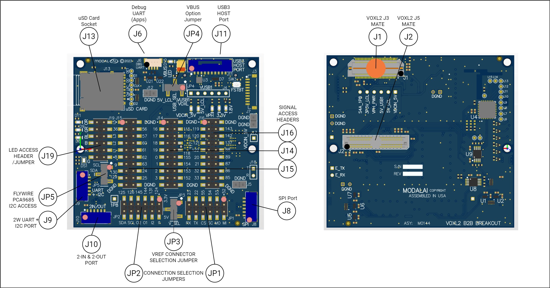
Overview Development Kits Schematics Dimensions 3D Drawings 2D Drawings Features Block Diagram Connector Callouts J1 - Legacy Voxl Debug/Expansion Port J2 - High Speed Board to Board Port J5, J7, J12 - GND Access Points J8 - SPI Port Connector J9 - UART + I2C Port Connector J10 - 2-In & 2-Out (2I/2O) Port Connector J11 - USB3 Host Port Connector J13 - uSD Card Socket JP1 - Connector Selection Jumper (1 of 2), SPI + UART JP2 - Connector Selection Jumper (2 of 2), 2I/2O + I2C JP3 - Port Connector J8, J9, J10 VTREF Selection Jumper JP4 - USB VBUS J11 Selection Jumper
PN Description MDK-M0144-00 VOXL 2 Developer Test Board only plus default jumpers and jumper wires MDK-M0144-01 Same as MDK-M0144-00, plus USB and UART cables (MCBL-00022-2, MCBL-00016-1, MCBL-00031-1)
.PDF SCH File
3D STEP
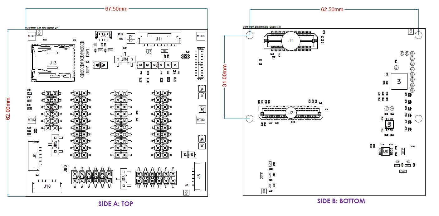
The 3D step only includes components that are populated (installed) as per the “-1_MAIN” design/build variant.
The 2D drawings shows all components whether populated or not. The MTG holes are arranged to align with the Voxl2 mounting hole pattern as shown.
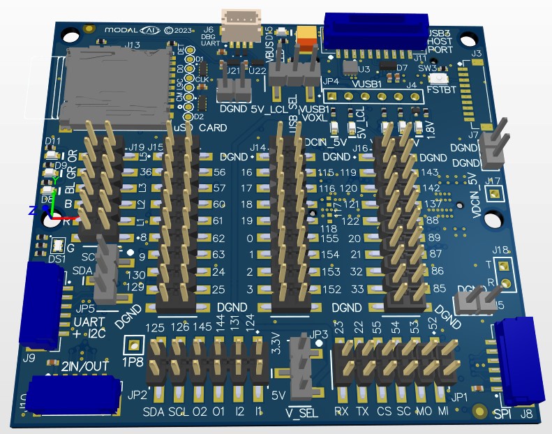
Quickly access ANY GPIO from J3 or J5 on large header pins (GND posts throughout the design) Remap any QUP port from J3 or J5 into an SPI, I2C, or UART function with direct on-board buffers/drivers mapped to standard JST Dronecode format cable connectors PCA9685 16-Channel I2C to PWM driver direct on board for PWM/LED development RGB LED plus discrete Orange, Green, and Blue LEDs for various/flexible indication or GPIO validation USB3 Host Port Linux Kernel (Apps) Debug UART Four (4) Mounting holes that align with Voxl2 mounting hole pattern Top
Warning: ONLY Change Jumper and Cable Connections while the entire system is Unpowered/OFF. Changing jumpers or fly-wires while powered will damage your B-Quad (M0144) and Voxl2
Connector MPN Board Connector QTH-030-01-L-D-A-K-TR Mating Connector https://docs.modalai.com/voxl2-connectors/#j3—legacy-board-to-board-connector-b2b
Color: Black
Pinouts as per Schematic and Voxl2 Mating Connector 1:1
Connector MPN Board Connector ADM6-30-01.5-L-4-2-A-TR Mating Connector https://docs.modalai.com/voxl2-connectors/#j5—high-speed-board-to-board-connector-hsb2b
Color: Black
Pinouts as per Schematic and Voxl2 Mating Connector 1:1
Connector MPN Board Connector BM10B-SRSS-TB(LF)(SN) Mating Connector SHR-10V-S-B
Color: Beige (DNI’d)
Pin Net M0144 Usage 1 VREG_S4A_1P8 1.8V I/O Rail VTREF 2 VPH_PWR 3.8V VREF 3 PM_RESIN_N Main PMIC RESET_N Signal (FASTBOOT) 4 APQ_RESOUT_LCL_N APQ Out of RESET Indication 5 QDL_H eDL Signal Input, LOW = eDL 6 WDOG_DIS_H Watchdog Disable Input 7 PMK8002_PMIC_CLK PMK8002 Spare Clock Output 8 PM8150L_AMUX1 PM8150L AMUX Input 9 PM8250_AMUX1 PM8250 AMUX Input 10 DGND System GND
Connector MPN Board Connector TSW-106-07-T-S Mating Connector M20-1060100
Color: Black (DNI’d)
Pin Net M0144 Usage 1 VDCIN_5V Raw Prime Input PTO/Access/Input (and J17.1) 2 VDC_5V_LOCAL eFuse Protected 5V Output Access 3 VDC_5V_USB1_VOXL Voxl2 5V USB Output Access 4 VPH_PWR Voxl2 3.8V VPH_PWR Access 5 VREG_3P3V_LOCAL Voxl2 3.3V Power Access 6 VREG_S4A_1P8 Voxl2 1.8V Power Access
Connector MPN Board Connector TSW-102-07-T-S Mating Connector M20-1060200
Color: Black
Pin Net M0144 Usage 1 DGND Probe GND Access 2 DGND Probe GND Access
Connector MPN Board Connector BM04B-SRSS-TB(LF)(SN) Mating Connector SHR-04V-S-B
Color: Beige
Pin Net M0144 Usage 1 VREG_3P3V_LOCAL Debug UART Signal Level VTREF 2 DEBUG_UART_RX Debug UART Receive (Input), 3.3V CMOS 3 DEBUG_UART_TX Debug UART Transmit (Output), 3.3V CMOS 4 DGND System GND
Connector MPN Board Connector SM06B-GHS-TB(LF)(SN) Mating Connector GHR-06V-S
Color: Beige
Pin Net M0144 Usage 1 V_SEL_CONNS Set by JP3 (3.3V or 5V) 2 SPI_MISO_3P3V_CON SPI Port J8 MISO, 3.3V CMOS 3 SPI_MOSI_3P3V_CON SPI Port J8 MOSI, 3.3V CMOS 4 SPI_SCLK_3P3V_CON SPI Port J8 SCLK, 3.3V CMOS 5 SPI_CS0_N_3P3V_CON SPI Port J8 CS0_N, 3.3V CMOS 6 DGND System GND
Top
Connector MPN Board Connector SM06B-GHS-TB(LF)(SN) Mating Connector GHR-06V-S
Color: Beige
Pin Net M0144 Usage 1 V_SEL_CONNS Set by JP3 (3.3V or 5V) 2 UART_TX_3P3V_CON UART+I2C Port J9 UART_TX, 3.3V CMOS 3 UART_RX_3P3V_CON UART+I2C Port J9 UART_RX, 3.3V CMOS 4 I2C_SDA_3P3V_CON UART+I2C Port J9 SDA, 3.3V CMOS 5 I2C_SCL_3P3V_CON UART+I2C Port J9 SCL, 3.3V CMOS 6 DGND System GND
Connector MPN Board Connector SM06B-GHS-TB(LF)(SN) Mating Connector GHR-06V-S
Color: Beige
Pin Net M0144 Usage 1 V_SEL_CONNS Set by JP3 (3.3V or 5V) 2 OUTPUT_1_3P3V_CON 2I/2O Port J10 OUTPUT_1, 3.3V CMOS 3 OUTPUT_2_3P3V_CON 2I/2O Port J10 OUTPUT_2, 3.3V CMOS 4 INPUT_1_3P3V_CON 2I/2O Port J10 INPUT_1, 3.3V CMOS 5 INPUT_2_3P3V_CON 2I/2O Port J10 INPUT_2, 3.3V CMOS 6 DGND System GND
Connector MPN Board Connector BM10B-GHS-TBT(LF)(SN)(N) Mating Connector GHR-10V-S
Color: Beige
Pin Net M0144 Usage 1 V_SEL_USB VBUS Set by JP4 (Voxl2 or eFuse sourced) 2 USB1_HS_CON_D_N Host Port USB_D- 3 USB1_HS_CON_D_P Host Port USB_D+ 4 DGND System GND 5 USB1_SS_RX_N Host Port SuperSpeed USB RX- 6 USB1_SS_RX_P Host Port SuperSpeed USB RX+ 7 DGND System GND 8 USB1_SS_TX_CONN_N Host Port SuperSpeed USB TX- 9 USB1_SS_TX_CONN_P Host Port SuperSpeed USB TX+ 10 DGND System GND
Connector MPN Board Connector DM3AT-SF-PEJM5
Color: Silver
Pinout as per uSD Standard. On-Board Test Points provided for each signal (see Schematic)
Connector MPN Board Connector TSM-110-01-L-DV Mating Connector Individual jumper wires PRT-12796 or similar
Note all Signal Breakout Access Headers have GND pins on 1, 2, 19, and 20 (the four corners)
Color: Black
Pin Net M0144 Usage 1 DGND System GND 2 DGND System GND 3 GPIO_16_QUP6_L0 GPIO# and QUP# as Indicated by net name 4 GPIO_115_I2C2_SDA GPIO# and QUP# as Indicated by net name 5 GPIO_17_QUP6_L1 GPIO# and QUP# as Indicated by net name 6 GPIO_116_I2C2_SCL GPIO# and QUP# as Indicated by net name 7 GPIO_18_QUP6_L2 GPIO# and QUP# as Indicated by net name 8 GPIO_117_QUP2_L2 GPIO# and QUP# as Indicated by net name 9 GPIO_19_QUP6_L3 GPIO# and QUP# as Indicated by net name 10 GPIO_118_QUP2_L3 GPIO# and QUP# as Indicated by net name 11 GPIO_0_QUP19_L0 GPIO# and QUP# as Indicated by net name 12 GPIO_155 GPIO# as Indicated by net name 13 GPIO_1_QUP19_L1 GPIO# and QUP# as Indicated by net name 14 GPIO_154 GPIO# as Indicated by net name 15 GPIO_2_QUP19_L2 GPIO# and QUP# as Indicated by net name 16 GPIO_153 GPIO# as Indicated by net name 17 GPIO_3_QUP19_L3 GPIO# and QUP# as Indicated by net name 18 GPIO_152 GPIO# as Indicated by net name 19 DGND System GND 20 DGND System GND
Top
Connector MPN Board Connector TSM-110-01-L-DV Mating Connector Individual jumper wires PRT-12796 or similar
Note all Signal Breakout Access Headers have GND pins on 1, 2, 19, and 20 (the four corners)
Color: Black
Pin Net M0144 Usage 1 DGND System GND 2 DGND System GND 3 GPIO_36_UART13_CTS GPIO# and QUP# as Indicated by net name 4 GPIO_56_I2C18_SDA GPIO# and QUP# as Indicated by net name 5 GPIO_37_UART13_RTS GPIO# and QUP# as Indicated by net name 6 GPIO_57_I2C18_SCL GPIO# and QUP# as Indicated by net name 7 GPIO_38_UART13_TXD GPIO# and QUP# as Indicated by net name 8 GPIO_60_QUP11_L0 GPIO# and QUP# as Indicated by net name 9 GPIO_39_UART13_RXD GPIO# and QUP# as Indicated by net name 10 GPIO_61_QUP11_L1 GPIO# and QUP# as Indicated by net name 11 GPIO_8_I2C4_SDA GPIO# and QUP# as Indicated by net name 12 GPIO_62_QUP11_L2 GPIO# and QUP# as Indicated by net name 13 GPIO_9_I2C4_SCL GPIO# and QUP# as Indicated by net name 14 GPIO_63_QUP11_L3 GPIO# and QUP# as Indicated by net name 15 GPIO_130_I2C10_SCL GPIO# and QUP# as Indicated by net name 16 GPIO_24_I2C8_SDA GPIO# and QUP# as Indicated by net name 17 GPIO_129_I2C10_SDA GPIO# and QUP# as Indicated by net name 18 GPIO_25_I2C8_SCL GPIO# and QUP# as Indicated by net name 19 DGND System GND 20 DGND System GND
Connector MPN Board Connector TSM-110-01-L-DV Mating Connector Individual jumper wires PRT-12796 or similar
Note all Signal Breakout Access Headers have GND pins on 1, 2, 19, and 20 (the four corners)
Color: Black
Pin Net M0144 Usage 1 DGND System GND 2 DGND System GND 3 GPIO_119_QUP3_L0 GPIO# and QUP# as Indicated by net name 4 GPIO_143 GPIO# as Indicated by net name 5 GPIO_120_QUP3_L1 GPIO# and QUP# as Indicated by net name 6 GPIO_142 GPIO# as Indicated by net name 7 GPIO_121_QUP3_L2 GPIO# and QUP# as Indicated by net name 8 GPIO_137 GPIO# as Indicated by net name 9 GPIO_122_QUP3_L3 GPIO# and QUP# as Indicated by net name 10 GPIO_88 GPIO# as Indicated by net name 11 GPIO_20_QUP7_L0 GPIO# and QUP# as Indicated by net name 12 GPIO_89 GPIO# as Indicated by net name 13 GPIO_21_QUP7_L1 GPIO# and QUP# as Indicated by net name 14 GPIO_87 GPIO# as Indicated by net name 15 GPIO_32_QUP12_L0 GPIO# and QUP# as Indicated by net name 16 GPIO_86 GPIO# as Indicated by net name 17 GPIO_33_QUP12_L1 GPIO# and QUP# as Indicated by net name 18 GPIO_85 GPIO# as Indicated by net name 19 DGND System GND 20 DGND System GND
Connector MPN Board Connector TSM-106-01-L-DV Mating Connector Individual jumper wires PRT-12796 or 2-pin jumpers
Color: Black
Pin Net M0144 Usage 1 LED0 Direct LED0 Output of PCA9685, 3.3V CMOS 2 LED_RGB_GREEN RGB Green Driver Input 1.8V <-> 5V CMOS 3 LED1 Direct LED1 Output of PCA9685, 3.3V CMOS 4 LED_RGB_RED RGB Red Driver Input 1.8V <-> 5V CMOS 5 LED2 Direct LED2 Output of PCA9685, 3.3V CMOS 6 LED_RGB_BLUE RGB Blue Driver Input 1.8V <-> 5V CMOS 7 LED3 Direct LED3 Output of PCA9685, 3.3V CMOS 8 LED_BLUE Discrete Blue LED Driver Input 1.8V <-> 5V CMOS 9 LED4 Direct LED4 Output of PCA9685, 3.3V CMOS 10 LED_GREEN Discrete Green LED Driver Input 1.8V <-> 5V CMOS 11 LED5 Direct LED5 Output of PCA9685, 3.3V CMOS 12 LED_ORANGE Discrete Orange LED Driver Input 1.8V <-> 5V CMOS
Top
Connector MPN Board Connector TSM-106-01-L-DV Mating Connector Individual jumper wires PRT-12796 or 2-pin jumpers
Color: Black
Pin Net M0144 Usage 1 GPIO_52_SPI17_MISO GPIO# and QUP# as Indicated by net name 2 SPI_MISO_SEL SPI MISO Selection Pin, Sets SPI Port J8 SW Mapping 3 GPIO_53_SPI17_MOSI GPIO# and QUP# as Indicated by net name 4 SPI_MOSI_SEL SPI MOSI Selection Pin, Sets SPI Port J8 SW Mapping 5 GPIO_54_SPI17_SCLK GPIO# and QUP# as Indicated by net name 6 SPI_SCLK_SEL SPI SCLK Selection Pin, Sets SPI Port J8 SW Mapping 7 GPIO_55_SPI17_CS GPIO# and QUP# as Indicated by net name 8 SPI_CS0_N_SEL SPI CS_N Selection Pin, Sets SPI Port J8 SW Mapping 9 GPIO_22_UART7_TXD GPIO# and QUP# as Indicated by net name 10 UART_TX_SEL UART TX Selection Pin, Sets UART Port J9 SW Mapping 11 GPIO_23_UART7_RXD GPIO# and QUP# as Indicated by net name 12 UART_RX_SEL UART RX Selection Pin, Sets UART Port J9 SW Mapping
Connector MPN Board Connector TSM-106-01-L-DV Mating Connector Individual jumper wires PRT-12796 or 2-pin jumpers
Color: Black
Pin Net M0144 Usage 1 GPIO_124 GPIO# as Indicated by net name 2 INPUT_1_SEL 2I/2O Port Selection Pin, Sets IN1 Port J10 SW Mapping 3 GPIO_131 GPIO# as Indicated by net name 4 INPUT_2_SEL 2I/2O Port Selection Pin, Sets IN2 Port J10 SW Mapping 5 GPIO_144 GPIO# as Indicated by net name 6 OUTPUT_1_SEL 2I/2O Port Selection Pin, Sets OUT1 Port J10 SW Mapping 7 GPIO_145 GPIO# as Indicated by net name 8 OUTPUT_2_SEL 2I/2O Port Selection Pin, Sets OUT2 Port J10 SW Mapping 9 GPIO_126_I2C9_SCL GPIO# and QUP# as Indicated by net name 10 I2C_SCL_SEL I2C SCL Selection Pin, Sets I2C Port J9 SW Mapping 11 GPIO_125_I2C9_SDA GPIO# and QUP# as Indicated by net name 12 I2C_SDA_SEL I2C SDA Selection Pin, Sets I2C Port J9 SW Mapping
Connector MPN Board Connector TSM-103-01-L-SV Mating Connector 2-pin jumper
Color: Black
Pin Net M0144 Usage 1 VREG_3P3V_LOCAL 3.3V Option for Connectors J8, J9, J10 2 V_SEL_CONNS Pin 1 VTREF for Connectors J8, J9, J10 3 VDC_5V_LOCAL 5V Option for Connectors J8, J9, J10
RED Jumper on Pins 1–2 or 2–3 ONLY, Default Shipped is 1–2 for ModalAI Compatability Switch to 2–3 for DroneCode Compatability
Top
Connector MPN Board Connector TSM-103-01-L-SV Mating Connector 2-pin jumper
Color: Black
Pin Net M0144 Usage 1 VDC_5V_USB1_VOXL VBUS Option, 2A limit, SW controlled by Voxl 2 GPIO_157 2 V_SEL_USB J11 USB VBUS, Pin 1 3 VDC_5V_LOCAL VBUS Option, 3A limit, direct from eFuse on Voxl 2
RED Jumper on Pins 1–2 or 2–3 ONLY, Default Shipped is 1–2 for Voxl2 SW controlled option at 2Amps Switch to 2–3 to bypass software control
Top
Connector MPN Board Connector TSM-103-01-L-SV Mating Connector Individual jumper wires PRT-12796
Color: Black
Pin Net M0144 Usage 1 I2C_SCL_PWM_LED_SEL I2C Bus SCL for PCA9685, 1.8V CMOS 2 I2C_SDA_PWM_LED_SEL I2C Bus SDA for PCA9685, 1.8V CMOS 3 DGND System GND
ONLY Connect I2C ports from 1.8V signals referenced to VREG_S4A_1P8, such as J14, J15, and J16. Do NOT connect from J9 signals. If an Aardvark type of device is required, be sure to use J20 VREG_S4A_1P8 as the VTREF of the host device so there are no power domain conflicts. Refer to the Schematic, Sheet 8, D1 for details.