Expansion Hardware Design Guide
Table of contents
This hardware design guide is intended for engineers who are comfortable designing and manufacturing custom PCBAs. The focus of this guide are PCBs that plug directly into a VOXL’s board to board connector. Details on VOXL 2’s board to board connector can be found on the VOXL 2 Connectors page.
VOXL 2 Custom Expansion PCB
An example add-on board for VOXL 2 with reference Altium schematic package can be downloaded here
For those without Altium, if you cannot get an online conversion or the 30-day trial period to work for you, here is another zip file of the generated outputs (SCH, BOM, 3D Step, ODB++, and an ASSY drawing with all relevant dimensions): Altium Generated Outputs
Note: When designing a custom expansion board, please be aware of these few pointers:
- We will review your schematic as a courtesy. Please reach out and we will coordinate so you are not posting your IP on a public facing portal/forum
- Not all GPIOs are created equal. There is a risk that some of your intended GPIO assignments may not work as expected.
- The Snapdragon SoC is a very complex chip with many cores in it. Some of these cores can “claim” GPIOs making them unavailable to the Linux kernel. We try to check for these ahead of time, but are not able to assess all possible combinations, so this Linux User Guide shows what has already been validated on various SW builds. If you contact us ahead of time, we can check specific ones and try to make sure the SW is ready for it or if your application should select a different GPIO/Port
- Explore this breakout board for J3 & J5 here for the best way to validate your desing before you tape-out.
Expansion Hardware Architecture
J3/J5 Expansion
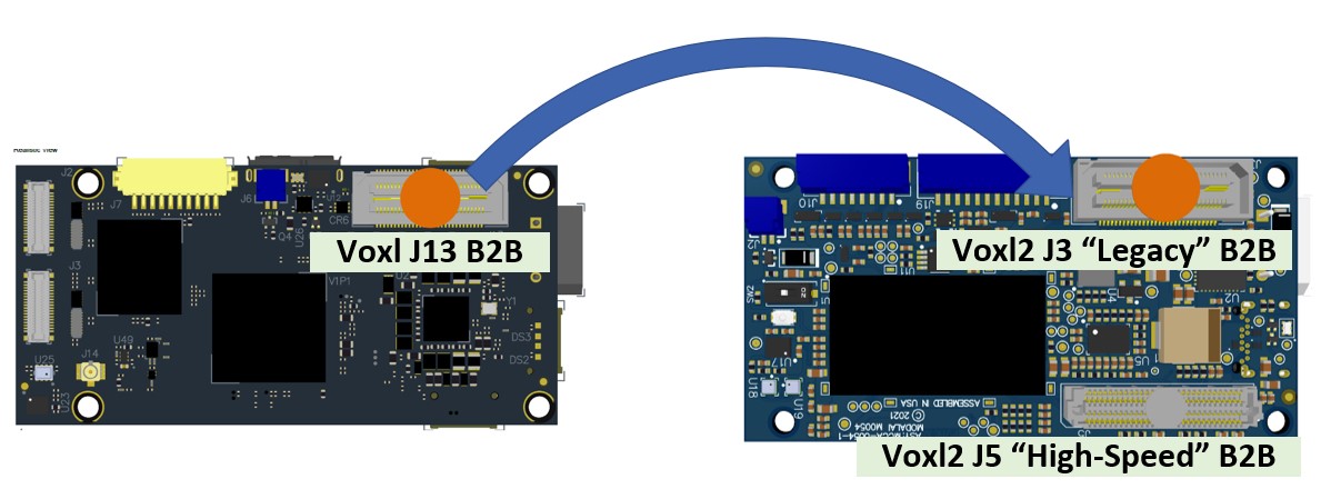
ModalAI designed the J3 (60-pin “Legacy B2B”) and J5 (120-pin “High-Speed B2B”) with many use cases in mind.
We took the success of the Voxl/Voxl-Flight 60-pin B2B (J13 in that board) used for LTE Modem and Microhard expansion, and took it to another level of expandability by incorporating J5. It is important to note that we explored using a 120-pin version of the same Samtec QSH/QTH series connector for this expansion, but we could not fit all of the incredible Voxl2 features we needed while doing so, so we had to use a higher density and different family of connectors from Samtec using the ADF/ADM line in order to meet all of the needs.
Please review these pinouts as needed: https://docs.modalai.com/voxl2-connectors/
- J3 on Voxl2 is in almost every way identical to J13 on Voxl. Any design that plugs into Voxl/Voxl-Flight J13, will electrically be safe to plug into Voxl2. All power and GND signals, along with critical debug and boot control signals map up (and the location of Voxl2’s mounting holes relative to J13 are the same relative to J3). So, if you bought a debug or fastboot adapter or LTE modem for Voxl/Voxl-Flight, it will still work exactly the same on Voxl2!!
- Just be careful to manage the potential contact of J5 to the bottom of your “legacy” board, such as M0048 (Microhard) where we have heard of instances of J5 pins contacting the bottom of the Microhard design, triggering a reset. We have a forum post on this where we recommend placing Kapton tape over J5 in these cases, and be sure to use 5mm standoffs between the boards to prevent any “diving board” issues.
- We made three key changes to J3 relative to J13
- We converted several sparsely used signals from J13 on Voxl into the USB3 Super-Speed signals to allow USB3 speeds on the Voxl2 platform with just J3 (no need for J5 in most USB expansion use-cases)
- We dedicated some of the former BLSP pins into an SPI and extra UART (see below for an explanation of QUPS)
- And the 5V Power (see next section)
5V Power IN vs 5V Power-Out
The 5V on pins 2, 4, and 6 are now dedicated as OUTPUT ONLY. On Voxl/Voxl-Flight, the direction of this power was loosely defined which allowed for some limited test boards to power Voxl. However, it was not designed for the 6A support Voxl2 really needs on power-up, so we came up with a different scheme for 5V as follows:
- J5 VDCIN_5V is 5V INPUT Only to the Voxl2 system (as an alternative to J4)
- J3 VDC_5V_LOCAL is 5V OUTPUT Only from the Voxl2 system.
Here is a diagram explaining our power system on Voxl2: 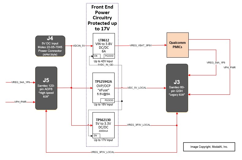
- If you try to power into J3, the board will not boot. It is protected by an eFuse that requires power in from J5 or J4 only.
- This eFuse validates the 5V input is within range (we can tolerate accidental insertion up to 12V “verified by test” and 17V “by design”), and there is no short downstream on the VDC_5V_LOCAL. Therefore, we will always recommend if your design provide power to Voxl2 VDCIN_5V on J5, then you should use the VDC_5V_LOCAL from J3 for your 5V peripherals, since you now have the confidence it is protected and guaranteed to be valid if present. Also note in the diagram, if the VDCIN_5V is not good, the eFuse keeps the primary “VBAT” power rail off, and the VREG_3P3V_LOCAL power OFF as well.
This decision does not impact any previous product from ModalAI, other than some of our own internal test hardware. So why did we do that?
We wanted to ensure customers had a reliable and clear way to treat Voxl2 as a “SOM” (System on Module) or to provide power from their dedicated Power Distribution Boards (PDB).
- In the case of a “SOM” approach, Voxl2 can be plugged into a host system via J3 and J5, and that host system will provide power to Voxl2 using J5 instead of the primary input connector J4.
- Voxl2 is still the main system component, but some customers do not want to use our Power Module, and are already designing a plug-in board, so there is an option to consolidate hardware by incorporating the power module functions directly into the expansion board.
Power Tap-Offs and their limits
As noted above, the 5V rail has special features that require attention. Additionally, we provide a range of other voltage options for your plug-in board, eliminating the need for additional power regulators—saving you effort, space, and cost. Refer to the diagram above to see the available voltages for plug-in boards:
- VREG_3P3V_LOCAL (3.3V)
- VPH_PWR (3.8V)
- VREG_S4A_1P8 (1.8V)
The table below illustrates the load limits for these voltage rails. These voltages are available at various connectors on VOXL 2, including the J3/J5 expansion, Camera Groups, and multiple JST connectors: 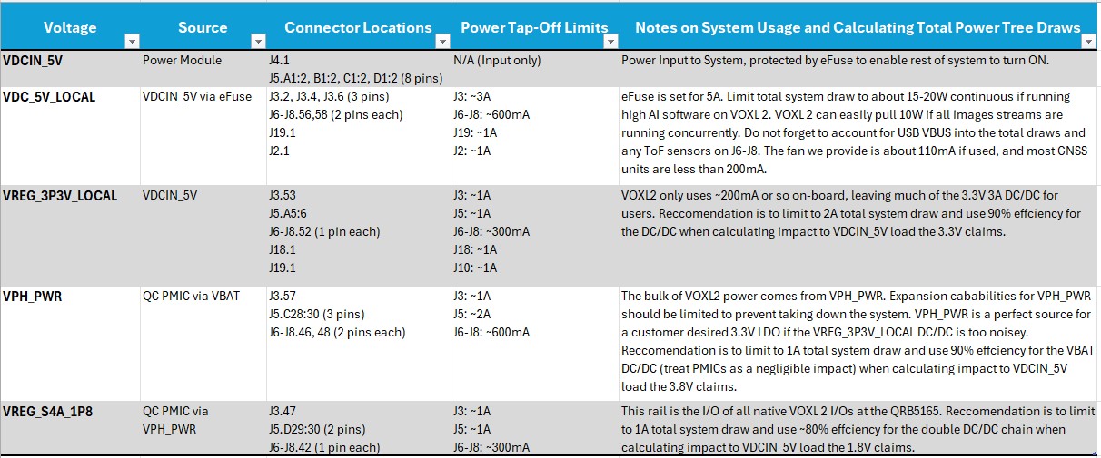
The convention for connector locations used in the table is “netlist” style, where J3.53 means connector J3 pin #53, and so on.
QUPS, The Key I/O Groups for Expansion
A QUP is a specific set of four GPIOs that have alternate functions underneath the hood enabling the group to work as an I2C bus, a UART port, or an SPI port. In total, there are 20 QUPs on the QRB5165. On Voxl2 and Voxl2-Mini we use many of them direct on-board, and make the rest of them available to customers for expansion purposes. The Software team has done a great job explaining how to use these in SW (and which ones are already enabled) in this section here: QUP Software
Understanding these QUPS and how to use them is paramount to your custom HW design’s success, so this section here should demystify how to use them correctly. When the group of GPIOs is assigned as a QUP (Qualcomm Universal Peripheral), it is assigned a “Lane” number, from 0:3. That lane number determines what function each GPIO maps to, according to the table shown here: 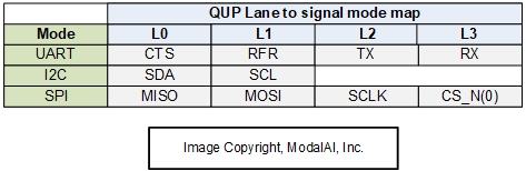
All users must be aware of a few key things and constraints for these QUPs:
- They are set in software through a “trust-zone” image, and therefore cannot be changed on-the-fly, for example from UART to SPI. If the platform image is set for SPI, it is always an SPI with that image.
- All QUPS are still fundamentally four GPIOs, so if a QUP is not needed, it is possible to use them as their primary GPIO (usually we indicate the GPIO # in the signals’s net name)
- Once a QUP is defined as one function, it can only be that function. For example, as shown in the table above, the I2C lines and 2W UART lines are distinct. On earlier versions of Qualcomm chipsets with BLSPs, this type of dual “2W UART + I2C” mode was possible. However, in the QRB5165, a QUP can only be a UART or only be an I2C, it cannot be both I2C + UART. I2C + 2-GPIOs is possible, and UART + 2-GPIOs is also possible.
- ModalAI does not support all possible combinations of QUPs. This would be a monumental task, and technically, this would have 4^20 possibilities. So please understand that we hope your application can work within our proven and validated modes as indicated on the software support page linked above.
- All Board to Board connector signals are at 1.8V. J3, J5, J6, J7, and J8 all have QUPS on them. Each one is always 1.8V natively and are direct to the QRB5165 without any buffers/translators. We provide VREG_S4A_1P8 (1.8V VDDIO) which is their VDD domain. This is useful for any voltage level translation needed to interface to 3.3V or 5V systems.
Here are a couple of examples of QUPs and how the hardware on Voxl2 defines them. This snapshot is from our brand-new “B-QUAD” Test Board (M0144) which will be available for sale soon. We will post all schematics and PCB info for this design making it a very valuable tool for all hardware and software developers. The B-QUAD will expose every GPIO, SD card signals, USB, and the Power signals and allow remapping to connectors set for either I2C, UART, SPI, or just plain GPI/GPOs. We even have an I2C to PWM device for RGB/LED/PWM control. Check back soon!! 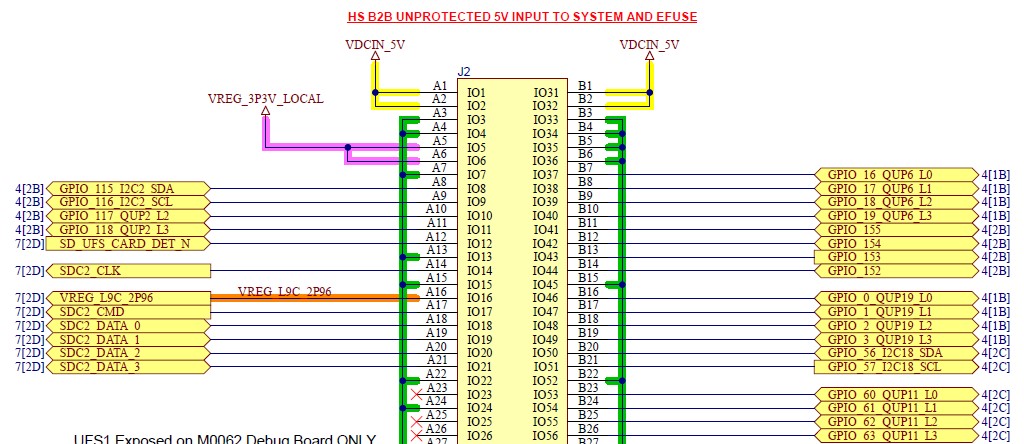 In the above image, we show a portion of the J5 mating connector on the B-QUAD. The pinout matches the previously linked Voxl2 connector pages. When ModalAI specifically identifies a QUP as a function, such as I2C or SPI, we like to include that as part of the name for clarity. Therefore, The conventions we follow for signal/net names is as follows:
- GPIO_xyz_(Function or QUP#)_(Lane or specific signal)
- GPIO_115_I2C2_SDA for example, is GPIO_115, and part of QUP2, and we expect it to be set as I2C, specifically SDATA
- GPIO_16_QUP6_L0 for example, is GPIO_16, and part of QUP6, and we have not explicitly defined it as a QUP, hence it is just defined as “Lane0” and can be either CTS, SDA, or MISO
- If a GPIO is not part of a QUP, we just list it as GPIO_xyz
- GPIO_153, GPIO_152, etc, are not part of a QUP, so they are just GPIOs (some may have other alternate functions which we can explain later).
- When we define a signal as I2C, we include a 2.2K-ohm pullup on Voxl2 to VREG_S4A_1P8. For example, the following I2C busses already have 2.2K pullups on Voxl2:
- QUP_2 (GPIO_115/116)
- QUP_4 (GPIO_8/9)
- QUP_8 (GPIO_24/25)
- QUP_9 (GPIO_125/126)
- QUP_10 (GPIO_129/130)
- QUP_18 (GPIO_56/57)
- If you need to define a generic QUP, or one defined already as a UART or SPI into an I2C, be sure to include pull-ups on your hardware design to VREG_S4A_1P8 before any translation buffers.
I2C Translation Important Note:
- All I2C ports on the JST Board-to-Cable connectors (J19 on VOXL 2 and VOXL 2 Mini plus ModalAI Plug-in Boards such as M00130 & M0090) use a TCA9517 to translate and buffer the I2C from the Snapdragon SOC 1.8V to 3.3V logic levels.
- The expectation is that these ports go directly to an accesory target device without further translation back down to lower voltages. For example; a micro-controller running at 3.3V native I/O levels. The TCA9517 cannot operate “B-port to B-port” and therefore if your system requires translating back down to lower voltages, such as 1.8V or 2.5V, a special un-buffered I2C translater will be required such as the PCA9306 or PCA9509.
- If you are designing a plug-in board and planning on using level translators to convert the 1.8V I2C signals to another voltage, please keep this important design constraint in-mind.
With all of the constraints applied to these QUPS, we always ask that you check the Linux User Guide and QUP Software pages often for your expected use case, and as always, contact us on the Forum for any clarification.
QUP I2C vs CCI_I2Cs
It is vitally important every user understands that the MIPI CSI I2C ports, referred to as CCI I2C ports, are not traditional QUPs. Do not plan on using a CCI_I2C bus for general purpose I2C usage. These I2C ports are specialized with direct access to the camera infrastructure, and cannot be executed as standard I2C ports through the Linux Kernel. The following signals noted in the Voxl2/Voxl2-Mini user guides are the signals dedicated as “CCI” I2C ports, and must only be used for image sensor applications:
- CCI_I2C0_SDA/SCL
- CCI_I2C1_SDA/SCL
- CCI_I2C2_SDA/SCL
- CCI_I2C3_SDA/SCL
These CCI I2C ports have VDDIO rails referenced to the power rail PM8009_VREG_L7_DOVDD_1P8 (J6-J8, pin 6). There are already 2.2K-Ohm pullups on Voxl2/Voxl2-Mini for these I2C ports.
USB EXPANSION OVER J3 & J5
The “secret sauce” to ModalAI Ecosystem expansion is based on USB over the J3 connector. Before starting off trying to design your own expansion (or for just a better understanding of our hardware designs), please review this section for how USB works on Voxl2, and how we use it to extend main-board support (Voxl/Voxl-Flight/Voxl2/Voxl2-Mini) to many radios and modems.
This is not intended to be an explanation of how USB works, but rather how we use USB in our hardware designs. If not already familiar with USB operations, please start with this basic wikipedia link then come back to review this section: https://en.wikipedia.org/wiki/USB
The Voxl2 USB Architecture is shown in this simple block diagram: 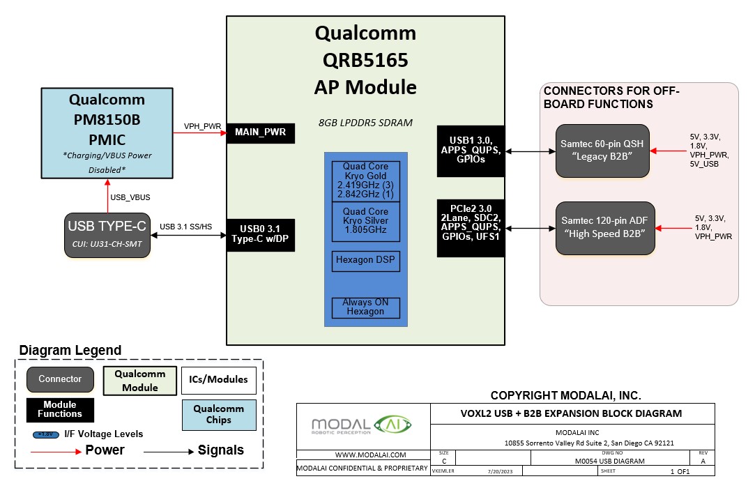
- USB-Type C (J9), which is the primary ADB/Programming Port for Voxl2 is seen on the left side going into the QRB5165’s USB-Port0.
- The charging functions of this port are disabled, which leads to a hardware limitation of it not supporting true OTG modes. This is why Voxl2 (M0054) is only capable of acting in peripheral mode
- We changed that on Voxl2-Mini (M0104) and are going to change that on a future spin of Voxl2 (TBD) so that it works in Host Mode
- The second USB port on the QRB5165 is shown on the top-right of the diagram, noted as USB1 3.0 (port 1, supports USB3.0 rates).
- As shown, this port, which operates exclusively in Host mode, is brought to the “Legacy” B2B connector J3.
From this foundational concept of the Host Only port residing on J3, it becomes clear how we achieve the bulk of our expansion using these B2B connectors.
ModalAI USB Hub Example
We will show an example hub architecture that we use on several designs. This will be useful to explain how we achieve the bus expansion and how we implement the various VBUS current limits throughout our diverse ecosystem of products. This will help any hardware designer learn how to match (or exceed) our designs where needed for your system constraints. We understand that not all system architecture constraints can be met with our designs, so with this knowledge of our implementation, you can enable your design to support what your system needs while maintaining compatibility in our ecosystem.
An example USB Hub Design from J3 is shown in this simple block diagram (you can see similar diagrams on our Microhard and 4G datasheet pages): 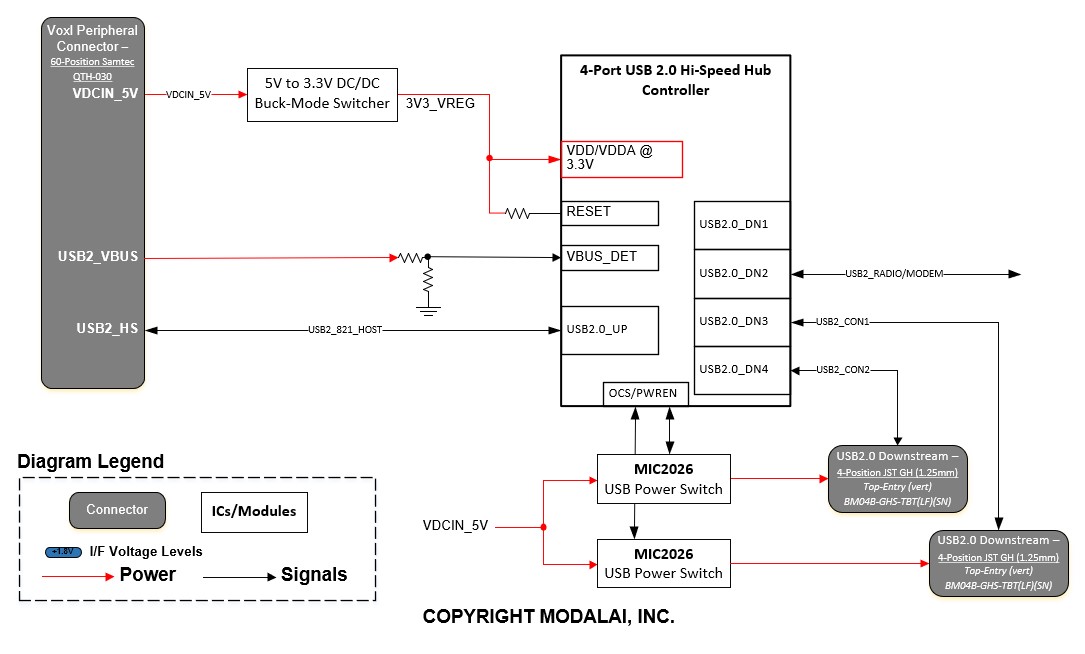
This block diagram shows these three key things vital to every USB hub based design:
1) Up-stream vs down-stream ports
2) VBUS detection
3) VBUS power delivery
- Note most importantly that the hub connects the up-stream facing port directly to J3. In this case, we only show USB2 for a Voxl/Voxl-Flight, but this applies to the USB3 lines from Voxl2 as well.
- On Voxl2, with USB3, make sure to connect the Hub TX to the Voxl2 port’s RX, and vice versa. You also need to include AC caps on BOTH RX/TX ports since there are no TX caps on Voxl2. Our M0144 expansion design schematic will illustrate this too.
- We already provide ESD protection and Common Mode filters on the USB2&3 lines on Voxl2, so there is no need to add in your own on the up-stream side. In fact, adding in more can break the interface.
- Do not want to use a Hub? No Problem, just bring the J3 signals VBUS, D+, D-, and a GND to a connector. Done. We do that on M0144 B-Quad test board.
- Next, note the hub’s VBUS detect. Every hub is different, but we use the VBUS from the J3 connector (divided down typically to meet 3.3V input levels) to indicate to the hub when it is time to enumerate. Every hub that we know of has an equivalent function, and it is important to use the VBUS from J3 for this purpose or enumeration with Voxl2 can be flakey or problematic.
- There are also various ways to issue a reset, and we provide a dedicated signal for USB_RESET that you can use if your application SW wants to trigger a hub reset. GPIO_131, as noted in the Connectors Page of Voxl2, is dedicated for this purpose. Please note it is an ACTIVE HIGH signal (HIGH = RESET) therefore, if your hub is active LOW, you will need to invert it. On our designs, we qualify this reset along with power good monitors to make sure reset is only released if power is good.
- All downstream ports are then capable of being brought to a connector as shown. These are how we cascade multiple USB peripherals from our plug-in boards.
- VBUS sourcing is also very important. Again, only you know your system constraints. We will do our best to communicate how our hardware works so you can determine if it meets your needs.
- The VBUS from Voxl2 is capable of sourcing 2A (Total). Even though the Samtec QSH/QTH pin specs are rated for 1A, we have a circuit on Voxl2 that can provide double that to that pin. You are free to use it as 2A as we do with extra thick routing right at each pin to help alleviate the 1A pin spec limit.
- If you need more than 2A, you can alternatively provide the 5V output from J3’s “VDC_5V_LOCAL” (shown as VDCIN_5V in the above diagram due to a Voxl1 based design, refer back above about the 5V input vs Output of Voxl1 vs Voxl2) and use that to source your VBUS.
- As shown in the diagram, we use dedicated USB power switches to provide VBUS power to each downstream connector. On all ModalAI hub based designs, every USB downstream port has a dedicated VBUS switch on it to set a limit and detect shorts or malfunctions on the port. We show a table just below that lists every design we have (so far) and for each port, what it’s VBUS limit is. Here is a zoom in image of that function for better clarity:
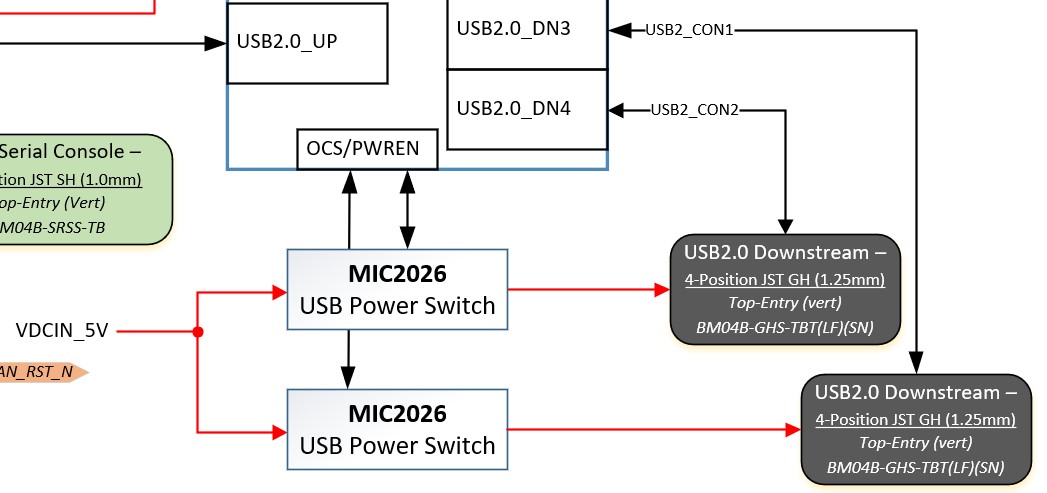
- As shown in the diagram, we use dedicated USB power switches to provide VBUS power to each downstream connector. On all ModalAI hub based designs, every USB downstream port has a dedicated VBUS switch on it to set a limit and detect shorts or malfunctions on the port. We show a table just below that lists every design we have (so far) and for each port, what it’s VBUS limit is. Here is a zoom in image of that function for better clarity:
- Fundamentally, on Voxl1/Voxl-Flight based designs, we limited this to a nominal USB2 port, with 500mA limits. On Voxl2, we increased that limit to support higher current devices (such as Boson, Doodle, etc) and made sure that every port is at least capable of delivering 1A at 5V.
- Voxl2-Mini is capable of providing 900mA on VBUS to match typical USB3 specs
- Make sure you review the device spec and application notes for your hub for how to implement power control switches. Most of them have minor nuances between them that can impact reliable operation.
This table shows a comprehensive listing of all our USB Hub Based designs and what the VBUS current limits are:
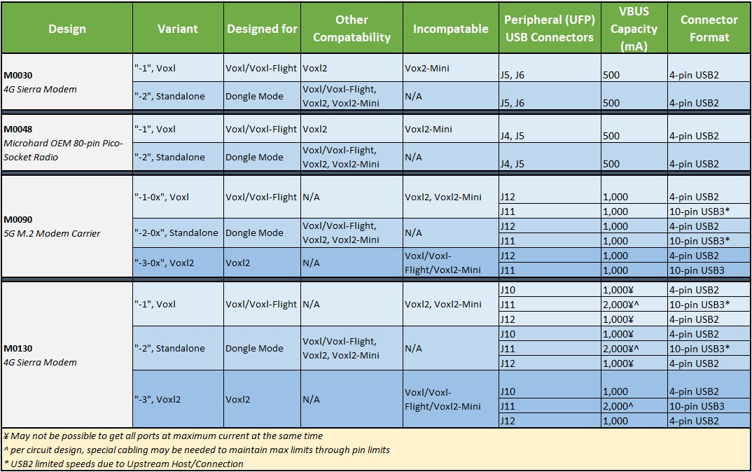 Please take note of the footnotes highlighting some limitations to these numbers. For example, not all ports can be maxed out at the same time, and if inherently the upstream port is USB2, the USB3 connectors will still enumerate as USB3 with the hub, but be bandwidth limited to the upstream host by USB2 speeds. The connector formats are referring to ModalAI’s designation of the 4-pin JST GH for USB3, and the 10-pin JST GH for USB3. The pinouts are indicated on each relevant design connector pages and are the same on all platforms (we never had an alternate USB pinout, nor will we).
PCIe using the High-Speed Board to Board (J5) Connector
VOXL 2 implements a 2-lane PCI Express (PCIe) interface compliant with PCIe Base Specification Revision 3.0, operating at a data rate of 8.0 GT/s (Gigatransfers per second) per lane.
Key Features:
- PCIe Gen 3.0 Compliance: Supports 8.0 GT/s data rate with efficient 128b/130b encoding.
- 2-Lane Configuration: Uses two transmit and two receive differential pairs, providing an aggregate bandwidth of 2 GB/s per direction.
- AC Coupling on TX Lines: Includes 0.22 µF AC coupling capacitors on TX (transmit) lines to ensure DC isolation and compatibility across varying device bias levels. These capacitors are placed close to the transmitters on VOXL 2 for optimal signal integrity.
- Note: When pairing VOXL 2 with a PCIe target device, be sure to check TX (Output) vs RX (input) directions. Some module vendors swap notations based on whether the HW is a host or target device. In these cases, it is easier to keep track of Inputs vs Outputs and make sure your design includes AC caps on your TX (Outputs) and connect to the VOXL 2 RX (Input) pins.
- REFCLK does not use AC caps as per PCIe Spec (the REFCLK is DC coupled), but systems requiring DC isolation may require it at your discretion.
- Impedance Control: All differential pairs are impedance-controlled to 85 ohms to ensure signal integrity and compliance with PCIe standards.
- Length Matching Requirements:
- _M/_P skew within each differential pair must be less than 0.7 mm.
- The length difference between the TX and RX signal paths must be within 20 mm to minimize timing mismatches.
- Signal Pinout: The PCI Express signal pinout follows the conventions specified in the ModalAI VOXL 2 J5 Connector Documentation
A simple block diagram showing the usage for PCIe is illustrated here: 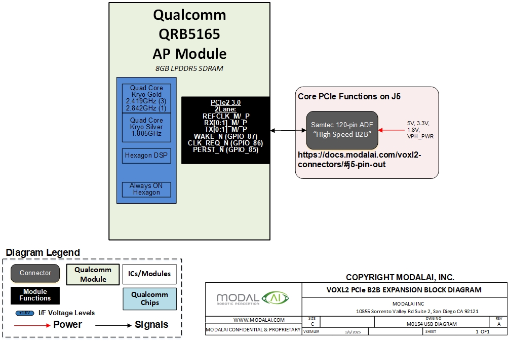
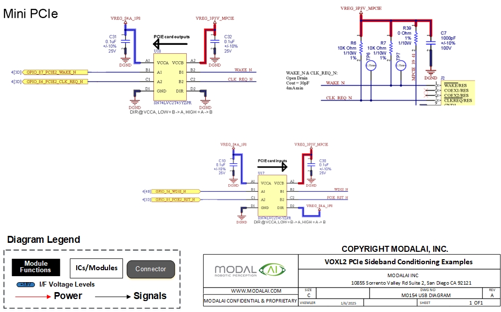
- Sideband GPIO Lines:
- WAKE_N (GPIO_87): Input to VOXL 2, used to signal wake-up events. This signal requires special consideration for voltage translation to ensure compatibility with VOXL 2’s input voltage levels.
- CLK_REQ_N (GPIO_86): Input to VOXL 2, serves as the clock request line for power management. Like WAKE_N, this signal also requires voltage translation to align with VOXL 2’s input requirements.
- PERST_N (GPIO_85): Output from VOXL 2, used to initialize the PCIe interface by resetting the target device. This signal requires signal translation to match the voltage requirements of the connected target device.
Important Note: VOXL 2 GPIOs operate on the VREG_S4A_1P8 power rail (1.8V). All buffer translation for WAKE_N, CLK_REQ_N, and PERST_N must use VREG_S4A_1P8 from the J5 connector to ensure proper voltage compatibility
The following example of sideband signal translation is directly from the ModalAI M0183 PCIe adapter design. Different parts or translation/isolation schemes may be required based on your target device, but in particular pay careful attention to open-drain and push-pull signal types and target voltage levels as listed in the corresponding specifications. Both M.2 and Mini-PCIe electro-mechanical specifications have allotments for module vendors to be flexible with certain I/O configurations and can impact your plug-in board’s functionality if not done correctly.
When planning on a PCIe based design, it is important your software team reaches out to us on the Forum for driver support verification. As of VOXL SDK version 1.4 there are very few supported PCIe devices for VOXL 2. You may need to plan on developing your own drivers for your targeted PCIe device.
If you have any questions about our designs, or how to make your own, contact us on the Forum.
** MUCH MORE TO COME, CHECK BACK OFTEN***