
VOXL 2 Connectors
Table of contents
- Video Overview of Connectors
- Connector Callouts
- Buttons
- Pinouts
- J2 - 5VDC Fan Control
- J3 - Legacy Board to Board Connector (B2B)
- J4 - Power Connector / I2C Battery Monitoring
- J5 - High Speed Board to Board Connector (HSB2B)
- Camera Group J6, J7, and J8 Pin-outs
- J10 - External SPI
- J18 UART (ESC)
- J19 - External Sensors (2x UART/ 2x I2C)
- I2C Important Note:
- Power Input/Output Important Note:
Video Overview of Connectors
Connector Callouts
Hover a connector to identify it — click to jump to its pinout.
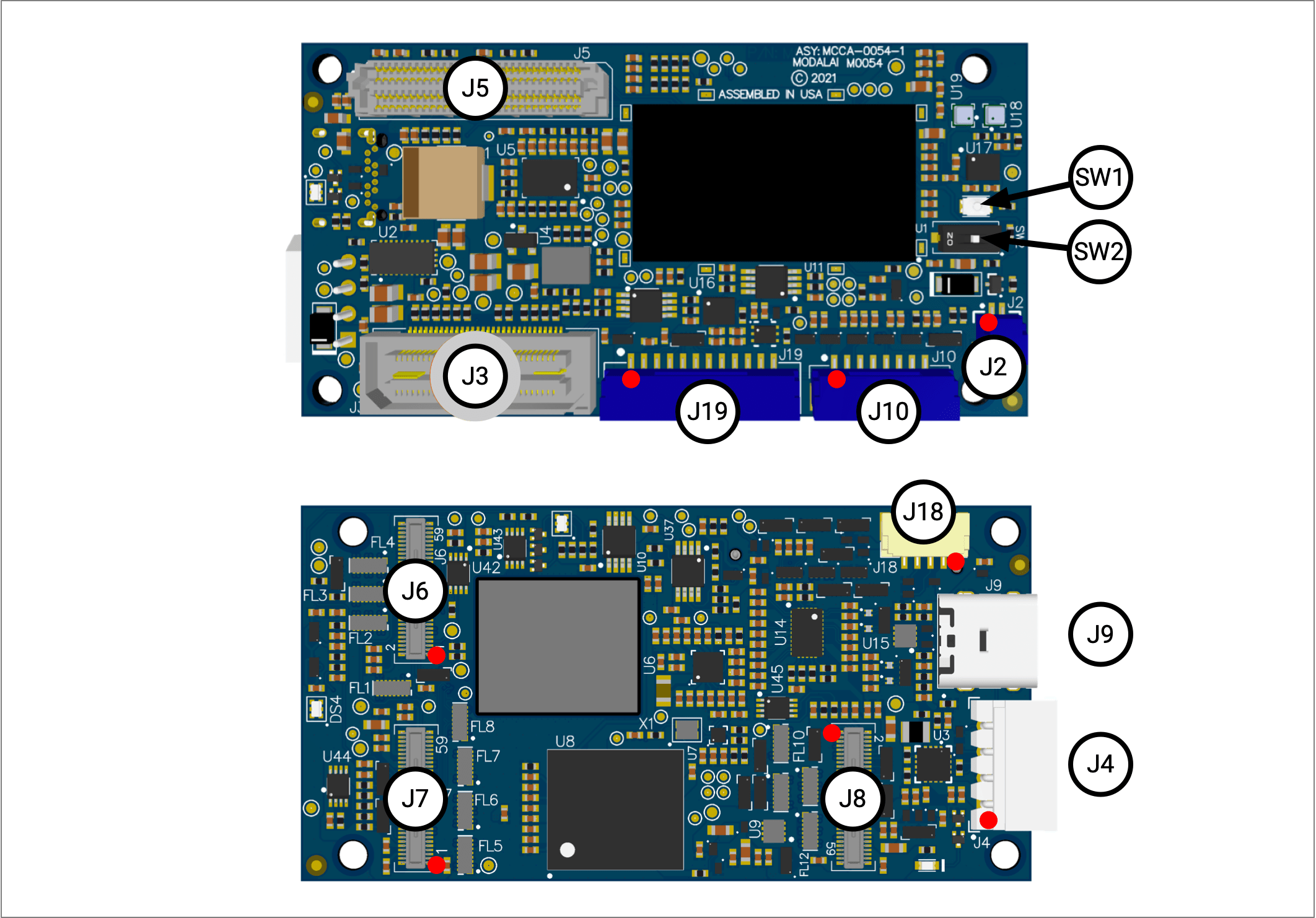
All single ended signals on B2B connectors J3, J5, J6, J7, and J8 are 1.8V CMOS unless explicitly noted. All single ended signals on cable-to-board connectors J10, J18, & J19 are 3.3V CMOS unless explicitly noted.
| Connector | Description | MPN (Board Side) | Mating MPN (Board/Cable Side) | Type | Signal Feature Summary |
|---|---|---|---|---|---|
| J2 | Fan | SM02B-SRSS-TB(LF)(SN) | SHR-02V-S | Cable Header, 2-pin R/A | 5V DC for FAN + PWM Controlled FAN-Return (GND) |
| J3 | Legacy B2B | QSH-030-01-L-D-K-TR | QTH-030-01-L-D-A-K-TR | B2B Receptacle, 60-pin | 5V/3.8V/3.3V/1.8V power for plug-in boards, JTAG and Debug Signals, QUP expansion, GPIOs, USB3.1 Gen 2 (USB1) |
| J4 | Prime Power In | 22057045 | 0050375043 | Cable Connector, 4-pin R/A | +5V main DC power in + GND, I2C@5V for power monitors |
| J5 | High Speed B2B | ADF6-30-03.5-L-4-2-A-TR | ADM6-30-01.5-L-4-2-A-TR | B2B Socket, 120-pin | More 3.8V/3.3V/1.8V power for plug-in boards, 5V power in for “SOM Mode”, QUP expansion, GPIOs, SDCC (SD Card V3.0), UFS1 (secondary UFS Flash), 2L PCIe Gen 3, AMUX and SPMI PMIC signals |
| J6 | Camera Group 0 | DF40C-60DP-0.4V(51) | DF40C-60DS-0.4V | B2B Plug, 60-pin | Qty-2 4L MIPI CSI ports, CCI and camera control signals, 8 power rails (from 1.05V up to 5V) for cameras and other sensors, dedicated SPI (QUP) port |
| J7 | Camera Group 1 | DF40C-60DP-0.4V(51) | DF40C-60DS-0.4V | B2B Plug, 60-pin | Qty-2 4L MIPI CSI ports, CCI and camera control signals, 8 power rails (from 1.05V up to 5V) for cameras and other sensors, dedicated SPI (QUP) port |
| J8 | Camera Group 2 | DF40C-60DP-0.4V(51) | DF40C-60DS-0.4V | B2B Plug, 60-pin | Qty-2 4L MIPI CSI ports, CCI and camera control signals, 8 power rails (from 1.05V up to 5V) for cameras and other sensors, dedicated SPI (QUP) port |
| J9 | USB-C (ADB) | UJ31-CH-3-SMT-TR | USB Type-C | Cable Receptacle, 24-pin R/A | ADB USB-C with re-driver and display port alternate mode (USB0) |
| J10 | SPI Expansion | SM08B-GHS-TB(LF)(SN) | GHR-08V-S | Cable Header, 8-pin R/A | SPI@3.3V with 2 CS_N pins, 32kHz CLK_OUT@3.3V |
| J18 | ESC (SLPI Access) | SM04B-GHS-TB(LF)(SN) | GHR-04V-S | Cable Header, 4-pin R/A | ESC UART@3.3V, 3.3V reference voltage |
| J19 | GNSS/MAG/RC/I2C (SLPI Access) | SM12B-GHS-TB(LF)(SN) | GHR-12V-S | Cable Header, 12-pin R/A | GNSS UART@3.3V, Magnetometer I2C@3.3V, 5V, RC UART, Spare I2C |
Add-on Board to Board Design Package
Reference add-on board Altium schematic package can be downloaded here
Buttons
SW1 - Force Fastboot Button
Force Fastboot momentary button.
To force device into fastboot mode:
- power off device, remove USB cable to completely power down
- press and hold SW1 button down
- power on device, attach USB cable
- release SW1 button
- from host computer, run
fastboot devicesand verify the device shows up. If not, restart this procedure
To reboot device to fastboot:
- device is powered on
- press and hold SW1 for 30 seconds until the device reboots into fastboot mode
SW2 - EDL Switch
Emergency Download switch, used for factory flashing. Should be left OFF. See user guide for QDL if interested in more information.
Pinouts
J2 - 5VDC Fan Control
| Pin # | Signal Name | Notes |
|---|---|---|
| 1 | VDC_5V_LOCAL | 5V protected power output * |
| 2 | FAN RETURN (GND) | Return limited to ~400mA |
J3 - Legacy Board to Board Connector (B2B)
Currently Supported Legacy Add-Ons:
- M0017 USB Debug Add-On
- M0030 LTE Modem Add-On
- M0048 Microhard Modem Add-On
The Legacy Board to Board connector is designed to host VOXL Add-ons such as the LTE Add-on v2 and the Microhard Add-on.
| Connector | MPN |
|---|---|
| Board Connector | QSH-030-01-L-D-K-TR |
| Mating Connector | QTH-030-01-L-D-A-K-TR |
J3 Pin-out
| Odd Pin # | Signal/Voltage | Even Pin # | Signal/Voltage |
|---|---|---|---|
| 1 | DGND | 2 | VDC_5V_LOCAL |
| 3 | GPIO_23_UART7_RXD, /dev/ttyHS1 | 4 | VDC_5V_LOCAL |
| 5 | GPIO_22_UART7_TXD, /dev/ttyHS1 | 6 | VDC_5V_LOCAL |
| 7 | GPIO_52_SPI17_MISO | 8 | USB1_HS_ID_LEGACY (Normally N.C.) |
| 9 | GPIO_53_SPI17_MOSI | 10 | DGND |
| 11 | DGND | 12 | USB1_HS_DM |
| 13 | GPIO_126_I2C9_SCL | 14 | USB1_HS_DP |
| 15 | GPIO_125_I2C9_SDA | 16 | VDC_5V_LOCAL_USB1 |
| 17 | GPIO_55_SPI17_CS | 18 | DGND |
| 19 | GPIO_54_SPI17_SCLK | 20 | USB1_SS_TX_M |
| 21 | DGND | 22 | USB1_SS_TX_P |
| 23 | GPIO_130_I2C10_SCL, /dev/i2c-1 | 24 | GPIO_20 |
| 25 | GPIO_129_I2C10_SDA, /dev/i2c-1 | 26 | GPIO_21 |
| 27 | GPIO_35_DBG_UART12_RX | 28 | GPIO_32_QUP12_L0 |
| 29 | GPIO_34_DBG_UART12_TX | 30 | GPIO_33_QUP12_L1 |
| 31 | DGND | 32 | USB1_SS_RX_M |
| 33 | JTAG_SRST_N | 34 | USB1_SS_RX_P |
| 35 | JTAG_TCK | 36 | DGND |
| 37 | JTAG_TDI | 38 | GPIO_131_USB_HUB_RESET |
| 39 | JTAG_TDO | 40 | GPIO_124 |
| 41 | JTAG_TMS | 42 | GPIO_145 |
| 43 | JTAG_TRST_N | 44 | DGND |
| 45 | JTAG_PS_HOLD | 46 | GPIO_90_FAST_BOOT_3 |
| 47 | VREG_S4A_1P8 | 48 | GPIO_76_FAST_BOOT_2 |
| 49 | PM_RESIN_N | 50 | GPIO_47_SPI14_CS2_FAST_BOOT_1 |
| 51 | SDM_RESOUT_N | 52 | GPIO_27_FAST_BOOT_0 |
| 53 | VREG_3P3V_LOCAL | 54 | GPIO_128_WDOG_DIS |
| 55 | KPD_PWR_N | 56 | SDM_FORCE_USB_BOOT |
| 57 | VPH_PWR | 58 | DGND |
| 59 | DGND | 60 | CLK_PMK_PMIC |
J4 - Power Connector / I2C Battery Monitoring
For use with VOXL Power Module
| Pin# | Signal | Notes/Usage |
|---|---|---|
| 1 | VDCIN_5V | DC from Power Module, “unprotected” |
| 2 | GND | Power Module Return |
| 3 | I2C_CLK | slpi_proc, SSC_QUP_1, 5V signal levels, Pullups on Power Module |
| 4 | I2C_SDA | slpi_proc, SSC_QUP_1, 5V signal levels, Pullups on Power Module |
Input Power Requirements
The VOXL Power Module provides the needed voltage and current demands of both VOXL (5V), VOXL 2 (5V), and VOXL 2 Mini (3.8V). It is a well tested and proven design.
For VOXL 2, we5V +/- 5% is expected to keep the eFuse happy. The VOXL Power Module is set for 5.08V at no-load to help compensate for any cable drops. 6A of in-rush support is required during power-on. The steady-state current requirement depends on your application and if a plug-in board (5G modem, Microhard, etc) is connected.
If you design with a 3A DC/DC, you will likely not be able to boot the system due to power on in-rush. Please use a 6A device for success with at least 188uF of bulk capacitance (qty-4 47uF for example) to match the VOXL Power Module performance.
If one needs to design their own power module, please submit a PCB review on our forum here
J5 - High Speed Board to Board Connector (HSB2B)
Currently Supported Add-Ons:
- M0062 - Debug/PCIe Add-On
- M0067 - 5G Add-On
- M0090 - 5G Add-On
| Connector | MPN |
|---|---|
| Board Connector | ADF6-30-03.5-L-4-2-A-TR |
| Mating Connector | ADM6-30-01.5-L-4-2-A-TR |
J5 Pin-out
| Pin | Signal/Voltage | Pin | Signal/Voltage | Pin | Signal/Voltage | Pin | Signal/Voltage |
|---|---|---|---|---|---|---|---|
| A1 (1) | VDCIN_5V | B1 (31) | VDCIN_5V | C1 (61) | VDCIN_5V | D1 (91) | VDCIN_5V |
| A2 | VDCIN_5V | B2 | VDCIN_5V | C2 | VDCIN_5V | D2 | VDCIN_5V |
| A3 | GND | B3 | GND | C3 | GND | D3 | GND |
| A4 | GND | B4 | GND | C4 | GND | D4 | GND |
| A5 | VREG_3P3V_LOCAL | B5 | GND | C5 | GPIO_119_SPI3_MISO | D5 | GPIO_36_UART13_CTS |
| A6 | VREG_3P3V_LOCAL | B6 | GND | C6 | GPIO_120_SPI3_MOSI | D6 | GPIO_37_UART13_RTS |
| A7 | GND | B7 | GPIO_16_QUP6_L0 | C7 | GPIO_121_SPI3_SCLK | D7 | GPIO_38_UART13_TXD |
| A8 | GPIO_115_I2C2_SDA | B8 | GPIO_17_QUP6_L1 | C8 | GPIO_122_SPI3_CS | D8 | GPIO_39_UART13_RXD |
| A9 | GPIO_116_I2C2_SCL | B9 | GPIO_18_QUP6_L2 | C9 | GPIO_24_I2C8_SDA | D9 | GPIO_8_I2C4_SDA |
| A10 | GPIO_117_QUP2_L2 | B10 | GPIO_19_QUP6_L3 | C10 | GPIO_25_I2C8_SCL | D10 | GPIO_9_I2C4_SCL |
| A11 | GPIO_118_QUP2_L3 | B11 | GPIO_155 | C11 | GND | D11 | PM8250_AMUX1 |
| A12 | SD_UFS_CARD_DET_N | B12 | GPIO_154 | C12 | GPIO_145 (intentional duplicate to Legacy B2B pin 42) | D12 | GND |
| A13 | GND | B13 | GPIO_153 | C13 | GPIO_144 | D13 | PCIE2_REFCLK_M |
| A14 | SDC2_CLK | B14 | GPIO_152 | C14 | GPIO_143 | D14 | PCIE2_REFCLK_P |
| A15 | GND | B15 | GND | C15 | GPIO_142 | D15 | GND |
| A16 | VREG_L9C_2P96 | B16 | GPIO_0_QUP19_L0 | C16 | GPIO_137 | D16 | PCIE2_RX0_M |
| A17 | SDC2_CMD | B17 | GPIO_1_QUP19_L1 | C17 | GND | D17 | PCIE2_RX0_P |
| A18 | SDC2_DATA_0 | B18 | GPIO_2_QUP19_L2, /dev/ttyHS2 | C18 | GPIO_88 | D18 | GND |
| A19 | SDC2_DATA_1 | B19 | GPIO_3_QUP19_L3, /dev/ttyHS2 | C19 | GPIO_89 | D19 | PCIE2_RX1_M |
| A20 | SDC2_DATA_2 | B20 | GPIO_56_I2C18_SDA | C20 | GPIO_87_PCIE2_WAKE_N | D20 | PCIE2_RX1_P |
| A21 | SDC2_DATA_3 | B21 | GPIO_57_I2C18_SCL | C21 | GPIO_86 | D21 | GND |
| A22 | GND | B22 | GND | C22 | GPIO_85 | D22 | PCIE2_TX0_M |
| A23 | UFS1_REFCLK | B23 | GPIO_60_QUP11_L0 | C23 | GND | D23 | PCIE2_TX0_P |
| A24 | GND | B24 | GPIO_61_QUP11_L1 | C24 | PMIC_8150L_AMUX1 | D24 | GND |
| A25 | UFS1_TX0_M | B25 | GPIO_62_QUP11_L2 | C25 | GND | D25 | PCIE2_TX1_M |
| A26 | UFS1_TX0_P | B26 | GPIO_63_QUP11_L3 | C26 | GND | D26 | PCIE2_TX1_P |
| A27 | GND | B27 | GND | C27 | GND | D27 | GND |
| A28 | UFS1_RX0_M | B28 | SPMI_CLK | C28 | VPH_PWR_3P8V | D28 | GND |
| A29 | UFS1_RX0_P | B29 | SPMI_DATA | C29 | VPH_PWR_3P8V | D29 | VREG_S4A_1P8 |
| A30 (30) | GND | B30 (60) | GND | C30 (90) | VPH_PWR_3P8V | D30 (120) | VREG_S4A_1P8 |
Camera Group J6, J7, and J8 Pin-outs
General Pin-out
Generic camera group pinout, please work with ModalAI for any mating designs to gauranteee proper operation
| Pin# | Signal |
|---|---|
| 1 | GND |
| 2 | GND |
| 3 | Lower CCI_I2C_SDA |
| 4 | DVDD 1.2V |
| 5 | Lower CCI_I2C_SCL |
| 6 | DOVDD 1.8V |
| 7 | GND |
| 8 | DVDD 1.05V |
| 9 | Lower CSI_CLK_P |
| 10 | Lower RST_N |
| 11 | Lower CSI_CLK_M |
| 12 | Lower MCLK |
| 13 | Lower CSI_DAT0_P |
| 14 | GND |
| 15 | Lower CSI_DAT0_M |
| 16 | Lower CCI Timer |
| 17 | GND |
| 18 | Upper CCI Timer |
| 19 | Lower CSI_DATA1_P |
| 20 | Upper MCLK |
| 21 | Lower CSI_DATA1_M |
| 22 | AVDD 2.8V |
| 23 | Lower CSI_DATA2_P |
| 24 | GND |
| 25 | Lower CSI_DATA2_M |
| 26 | Upper RST_N, Shared |
| 27 | GND |
| 28 | Upper CCI_I2C_SDA |
| 29 | Lower CSI_DATA3_P |
| 30 | Upper CCI_I2C_SCL |
| 31 | Lower CSI_DATA3_M |
| 32 | Spare MCLK/GPIO |
| 33 | GND |
| 34 | Group SPI MISO (groups 0/1) |
| 35 | Upper CSI_CLK_P |
| 36 | Group SPI MOSI (groups 0/1) |
| 37 | Upper CSI_CLK_M |
| 38 | Group SPI SCLK (groups 0/1) |
| 39 | Upper CSI_DATA0_P |
| 40 | Group SPI CS_N (groups 0/1) |
| 41 | Upper CSI_DATA0_M |
| 42 | VREG_S4A_1P8 |
| 43 | GND |
| 44 | GND |
| 45 | Upper CSI_DATA1_P |
| 46 | VPH_PWR 3.8V |
| 47 | Upper CSI_DATA1_M |
| 48 | VPH_PWR 3.8V |
| 49 | Upper CSI_DATA2_P |
| 50 | GND |
| 51 | Upper CSI_DATA2_M |
| 52 | 3.3V |
| 53 | GND |
| 54 | GND |
| 55 | Upper CSI_DATA3_P |
| 56 | 5V |
| 57 | Upper CSI_DATA3_M |
| 58 | 5V |
| 59 | GND |
| 60 | GND |
J6 - Camera Group 0 Specific Pinout
Configured for the following hardware:
                                                 +--> M0010
- M0054 J6 <--> M0076-1 interposer <--> M0010 <--|
                                                 +--> M0010
More camera information here
Connector: DF40C-60DP-0.4V(51)
Device Tree:
qcom,cam-sensor0qcom,cam-sensor1
J6 Pin-out
| Pin # | Signal Name | Usage / Notes |
|---|---|---|
| 1 | GND | |
| 2 | GND | |
| 3 | CCI_I2C0_SDA | CAM0_CCI0_SDA, gpio101 |
| 4 | VREG_PM8009_L2_1P2 | DVDD 1.2V |
| 5 | CCI_I2C0_SCL | CAM0_CCI0_SCL, gpio102 |
| 6 | VREG_PM8009_L7_1P8 | CAM0_VIO_1P8, CAM0_VIO_1P8 |
| 7 | GND | |
| 8 | VREG_PM8009_L1_1P05 | CAM0_VDD_1P05, NOTE: current this is ~1.13VDC |
| 9 | CSI0_CLK_CON_P | |
| 10 | GPIO_93_CAM0_RST_N | CAM0_RST_N, gpio93 |
| 11 | CSI0_CLK_CON_N | |
| 12 | GPIO_94_CAM_MCLK0_CON | CAM_MCLK0_CON, gpio94 |
| 13 | CSI0_LANE0_CON_P | LEFT |
| 14 | GND | |
| 15 | CSI0_LANE0_CON_N | LEFT |
| 16 | GPIO_110_CCI_TIMER1 | (unused in version 0) |
| 17 | GND | |
| 18 | GPIO_113_CCI_TIMER4 | CAM_FSYNC_1_OUT, CAM_FSYNC0_IN |
| 19 | CSI0_LANE1_CON_P | RIGHT |
| 20 | CAM_MCLK1_CON | CAM_MCLK1_CON, gpio95 |
| 21 | CSI0_LANE1_CON_N | RIGHT |
| 22 | VREG_PM8009_L5_2P8 | CAM0_AVDD_2P8, CAM1_AVDD_2P8 |
| 23 | CSI0_LANE2_CON_P | |
| 24 | GND | |
| 25 | CSI0_LANE2_CON_N | |
| 26 | GPIO_109_CAM3_RST_N | (shared, CAM3_RST_N) |
| 27 | GND | |
| 28 | CCI_I2C1_SDA | CAM1_CCI1_SDA, CAM4_CCI1_SDA |
| 29 | CSI0_LANE3_CON_P | |
| 30 | CCI_I2C1_SCL | CAM1_CCI1_SCL, CAM4_CCI1_SCL |
| Pin # | Signal Name | Notes |
|---|---|---|
| 31 | CSI0_LANE3_CON_N | |
| 32 | MCLK6_G0_CON | (shared) CAM1_RST_N, gpio100, |
| 33 | GND | |
| 34 | GPIO_28_CAM0_SPI0_MISO | /dev/spidev0.0 |
| 35 | CSI1_CLK_CON_P | |
| 36 | GPIO_29_CAM0_SPI0_MOSI | /dev/spidev0.0 |
| 37 | CSI1_CLK_CON_N | |
| 38 | GPIO_30_CAM0_SPI0_CLK | /dev/spidev0.0 |
| 39 | CSI1_LANE0_CON_P | |
| 40 | GPIO_31_CAM0_SPI0_CS | /dev/spidev0.0 |
| 41 | CSI1_LANE0_CON_N | |
| 42 | VREG_S4A_1P8 | |
| 43 | GND | |
| 44 | GND | |
| 45 | CSI1_LANE1_CON_P | |
| 46 | VPH_PWR | |
| 47 | CSI1_LANE1_CON_N | |
| 48 | VPH_PWR | |
| 49 | CSI1_LANE2_CON_P | |
| 50 | GND | |
| 51 | CSI1_LANE2_CON_N | |
| 52 | VREG_3P3V_LOCAL | |
| 53 | GND | |
| 54 | GND | |
| 55 | CSI1_LANE3_CON_P | |
| 56 | VDC_5V_LOCAL | |
| 57 | CSI1_LANE3_CON_N | |
| 58 | VDC_5V_LOCAL | |
| 59 | GND | |
| 60 | GND |
J7 - Camera Group 1 Specific Pinout
Configured for the following hardware:
                                +--> M0014   (M0084-JL - lower)
- M0054 J7 <--> M0084 flex <----|
                                +--> M0025-2 (M0084-JU - upper)
Connector: DF40C-60DP-0.4V(51)
Device Tree:
qcom,cam-sensor2qcom,cam-sensor3
J7 Pin-out
| Pin # | Signal Name | Usage / Notes |
|---|---|---|
| 1 | GND | |
| 2 | GND | |
| 3 | CCI_I2C2_SDA | CAM2_CCI2_SDA, gpio105 |
| 4 | VREG_PM8009_L2_1P2 | (M0084, R1 not stuffed, not routed) |
| 5 | CCI_I2C2_SCL | CAM2_CCI2_SCL, gpio106 |
| 6 | VREG_PM8009_L7_1P8 | CAM2_DOVDD_1P8, CAM3_DOVDD_1P8 |
| 7 | GND | |
| 8 | VREG_PM8009_L1_1P05 | (M0084, R2 stuffed) CAM2_VDD_1P05,CAM3_VDD_1P05 (NOTE: current this is ~1.13VDC) |
| 9 | CSI2_CLK_CON_P | |
| 10 | GPIO_92_CAM1_RST_N | RST_LOWER_N, gpio92 |
| 11 | CSI2_CLK_CON_N | |
| 12 | GPIO_96_CAM_MCLK2 | MCLK_LOW, gpio96 |
| 13 | CSI2_LANE0_CON_P | |
| 14 | GND | |
| 15 | CSI2_LANE0_CON_N | |
| 16 | GPIO_111_CCI_TIMER2 | CCI_TIMER_LOWER |
| 17 | GND | |
| 18 | GPIO_114_CCI_ASYNC_IN | CCI_TIMER_UPPER (Do Not Use on M0054 Voxl2, there is a HW limitation impacting this pin. It will be fixed on future HW. Voxl2 Mini is not impacted by this issue.) |
| 19 | CSI2_LANE1_CON_P | |
| 20 | GPIO97_CAM_MCLK3_CON | MCLK_UPPER, gpio97 |
| 21 | CSI2_LANE1_CON_N | |
| 22 | VREG_PM8009_L6_2P8 | AVDD_2P8, CAM2_DOVDD_2P8, CAM3_DOVDD_2P8 |
| 23 | CSI2_LANE2_CON_P | |
| 24 | GND | |
| 25 | CSI2_LANE2_CON_N | |
| 26 | GPIO_109_CAM3_RST_N | (shared, RST_UPPER_SHARED_N) |
| 27 | GND | |
| 28 | CCI_I2C3_SDA | CAM3_CCI3_SDA, CAM5_CCI3_SDA, gpio107 |
| 29 | CSI2_LANE3_CON_P | |
| 30 | CCI_I2C3_SCL | CAM3_CCI3_SCL, CAM5_CCI3_SCL, gpio108 |
| Pin # | Signal Name | Notes |
|---|---|---|
| 31 | CSI2_LANE3_CON_N | |
| 32 | MCLK6_G1_CON | (shared) GPIO_MCLK6_SHARED, gpio100 |
| 33 | GND | |
| 34 | GPIO_4_CAM1_SPI1_MISO | GPIO_4, /dev/spidev1.0 can be enabled in DT, see this commit to see how to re-enable if needed. |
| 35 | CSI3_CLK_CON_P | |
| 36 | GPIO_5_CAM1_SPI1_MOSI | GPIO_5, /dev/spidev1.0 can be enabled in DT see this commit to see how to re-enable if needed. |
| 37 | CSI3_CLK_CON_N | |
| 38 | GPIO_6_CAM1_SPI1_CLK | GPIO_6, /dev/spidev1.0 can be enabled in DT see this commit to see how to re-enable if needed. |
| 39 | CSI3_LANE0_CON_P | |
| 40 | GPIO_7_CAM1_SPI1_CS | GPIO_7, /dev/spidev1.0 can be enabled in DT see this commit to see how to re-enable if needed. |
| 41 | CSI3_LANE0_CON_N | |
| 42 | VREG_S4A_1P8 | |
| 43 | GND | |
| 44 | GND | |
| 45 | CSI3_LANE1_CON_P | |
| 46 | VPH_PWR | |
| 47 | CSI3_LANE1_CON_N | |
| 48 | VPH_PWR | |
| 49 | CSI3_LANE2_CON_P | |
| 50 | GND | |
| 51 | CSI3_LANE2_CON_N | |
| 52 | VREG_3P3V_LOCAL | |
| 53 | GND | |
| 54 | GND | |
| 55 | CSI3_LANE3_CON_P | |
| 56 | VDC_5V_LOCAL | |
| 57 | CSI3_LANE3_CON_N | |
| 58 | VDC_5V_LOCAL | |
| 59 | GND | |
| 60 | GND |
J8 - Camera Group 2 Specific Pinout
Configured for the following hardware:
                                                 +--> M0010
- M0054 J8 <--> M0076-1 interposer <--> M0010 <--|
                                                 +--> M0010
More camera information here
Connector: DF40C-60DP-0.4V(51)
Device Tree:
qcom,cam-sensor4qcom,cam-sensor5
J8 Pin-out
| Pin # | Signal Name | Usage / Notes |
|---|---|---|
| 1 | GND | |
| 2 | GND | |
| 3 | CCI_I2C1_SDA | CAM1_CCI1_SDA, CAM4_CCI1_SDA, gpio103 |
| 4 | VREG_PM8009_L2_1P2 | DVDD 1.2V |
| 5 | CCI_I2C1_SCL | CAM1_CCI1_SCL, CAM4_CCI1_SCL gpio104 |
| 6 | VREG_PM8009_L7_1P8 | CAM0_VIO_1P8, CAM0_VIO_1P8 |
| 7 | GND | |
| 8 | VREG_PM8009_L1_1P05 | CAM0_VDD_1P05, NOTE: current this is ~1.13VDC |
| 9 | CSI4_CLK_CON_P | |
| 10 | GPIO_78_CAM4_RST_N | CAM4_RST_N, gpio78 |
| 11 | CSI4_CLK_CON_N | |
| 12 | GPIO_98_CAM_MCLK4 | CAM_MCLK4_CON, gpio98 |
| 13 | CSI4_LANE0_CON_P | LEFT |
| 14 | GND | |
| 15 | CSI4_LANE0_CON_N | LEFT |
| 16 | GPIO_112_CCI_TIMER3 | (unused in version 0) |
| 17 | GND | |
| 18 | GPIO_111_CCI_TIMER2 | CAM_FSYNC_5_OUT, CAM_FSYNC4_IN |
| 19 | CSI4_LANE1_CON_P | RIGHT |
| 20 | CAM_MCLK5_CON | CAM_MCLK5_CON, gpio99 |
| 21 | CSI4_LANE1_CON_N | RIGHT |
| 22 | VREG_PM8009_L6_2P8 | CAM4_AVDD_2P8, CAM5_AVDD_2P8 |
| 23 | CSI4_LANE2_CON_P | |
| 24 | GND | |
| 25 | CSI4_LANE2_CON_N | |
| 26 | GPIO_109_CAM3_RST_N | (shared, CAM3_RST_N) |
| 27 | GND | |
| 28 | CCI_I2C3_SDA | CAM5_CCI3_SDA, CAM3_CCI3_SDA, gpio107 |
| 29 | CSI4_LANE3_CON_P | |
| 30 | CCI_I2C3_SCL | CAM5_CCI3_SCL, CAM3_CCI3_SCL, gpio108 |
| Pin # | Signal Name | Notes |
|---|---|---|
| 31 | CSI4_LANE3_CON_N | |
| 32 | MCLK6_G2_CON | (shared) GPIO_MCLK6_SHARED, gpio100 |
| 33 | GND | |
| 34 | GPIO_12_CAM2 | Not used as RTS, not available as GPIO |
| 35 | CSI5_CLK_CON_P | |
| 36 | GPIO_13_CAM2 | Not used as CTS, not available as GPIO |
| 37 | CSI5_CLK_CON_N | |
| 38 | GPIO_14_CAM2_UART5_TX | /dev/ttyHS0 |
| 39 | CSI5_LANE0_CON_P | |
| 40 | GPIO_15_CAM2_UART5_RX | /dev/ttyHS0 |
| 41 | CSI5_LANE0_CON_N | |
| 42 | VREG_S4A_1P8 | |
| 43 | GND | |
| 44 | GND | |
| 45 | CSI5_LANE1_CON_P | |
| 46 | VPH_PWR | |
| 47 | CSI5_LANE1_CON_N | |
| 48 | VPH_PWR | |
| 49 | CSI5_LANE2_CON_P | |
| 50 | GND | |
| 51 | CSI5_LANE2_CON_N | |
| 52 | VREG_3P3V_LOCAL | |
| 53 | GND | |
| 54 | GND | |
| 55 | CSI5_LANE3_CON_P | |
| 56 | VDC_5V_LOCAL | |
| 57 | CSI5_LANE3_CON_N | |
| 58 | VDC_5V_LOCAL | |
| 59 | GND | |
| 60 | GND |
J10 - External SPI
Overview
Available from apps proc as /dev/spidev14.0. J10 Achieved feature parity with VOXL 2 Mini when the design was updated from M0054 -> M0154. It is capable of either UART or SPI based on GPIO_67 control, but fixed in the Kernel for that build (not dynamic)
J10 Pin-out, SPI Mode (Fixed), M0054
| Pin# | Signal | Notes/Usage |
|---|---|---|
| 1 | VREG_3P3V_LOCAL | 3.3V Power Output * |
| 2 | MISO (Input) | APPS_QUP_14, 3.3V signal levels |
| 3 | MOSI (Output) | APPS_QUP_14, 3.3V signal levels |
| 4 | SCLK (Output) | APPS_QUP_14, 3.3V signal levels |
| 5 | CS0_N (Output) | APPS_QUP_14, 3.3V signal levels |
| 6 | CS1_N/GPIO_46 (Output) | Second SPI CS_N or GPIO |
| 7 | 32K_CLK_OUT (Output) | 32kHz PMIC Sleep CLK, 3.3V signal levels |
| 8 | GND | GND |
J10 Pin-out, SPI Mode (GPIO_67 = HIGH), M0154
| Pin# | Signal | Notes/Usage |
|---|---|---|
| 1 | VREG_3P3V_LOCAL | 3.3V Power Output * |
| 2 | MISO (Input) | APPS_QUP_14, 3.3V signal levels |
| 3 | MOSI (Output) | APPS_QUP_14, 3.3V signal levels |
| 4 | SCLK (Output) | APPS_QUP_14, 3.3V signal levels |
| 5 | CS0_N (Output) | APPS_QUP_14, 3.3V signal levels |
| 6 | CS1_N/GPIO_46 (Output) | Second SPI CS_N or GPO |
| 7 | GPIO_64_INT (Input) | GPIO_64 as input for INT, 3.3V signal levels |
| 8 | GND | GND |
J10 Pin-out, UART Mode (GPIO_67 = LOW), M0154
| Pin# | Signal | Notes/Usage |
|---|---|---|
| 1 | VREG_3P3V_LOCAL | 3.3V Power Output * |
| 2 | GPIO_40 (Input) | GPIO_40 Input, 3.3V signal levels |
| 3 | GPIO_41 (Output) | GPIO_41 Output, 3.3V signal levels |
| 4 | UART_14_TX (Output) | APPS_QUP_14, 3.3V signal levels |
| 5 | UART_14_RX (Input) | APPS_QUP_14, 3.3V signal levels |
| 6 | GPIO_46 (Input) | GPIO_46 as input, 3.3V signal levels |
| 7 | GPIO_64_INT (Input) | GPIO_64 as input for INT, 3.3V signal levels |
| 8 | GND | GND |
J18 UART (ESC)
J18 ESC UART
| Pin# | Signal | Notes/Usage |
|---|---|---|
| 1 | VREG_3P3V_LOCAL | 3.3V Power Output * |
| 2 | ESC_UART_TX (Output) | slpi_proc, SSC_QUP_2, 3.3V signal levels. |
| 3 | ESC_UART_RX (Input) | slpi_proc, SSC_QUP_2, 3.3V signal levels. |
| 4 | GND | GND |
SW Summary
Available from DSP as QUP2. In the factory configuration, PX4 communicates to the VOXL ESC through this UART.
J19 - External Sensors (2x UART/ 2x I2C)
J19 Pin-out
| Pin # | Signal Name | Notes |
|---|---|---|
| 1 | VDC_5V_LOCAL | GNSS/Mag power * |
| 2 | GNSS TX 3P3V | slpi_proc, SSC_QUP6 |
| 3 | GNSS RX 3P3V | slpi_proc, SSC_QUP6 |
| 4 | MAG SCL 3P3V | slpi_proc, SSC_QUP0 |
| 5 | MAG SDA 3P3V | slpi_proc, SSC_QUP0 |
| 6 | GND | |
| 7 | I2C3 SDA 3P3V | slpi_proc, SSC_QUP3 |
| 8 | I2C3 SCL 3P3V | slpi_proc, SSC_QUP3 |
| 9 | VREG_3P3V_RC | RC power *, controllable via GPIO 159 |
| 10 | RC_UART_TX (Output) | slpi_proc, SSC_QUP7, 3.3V signal levels |
| 11 | RC_UART_RX (Input) | slpi_proc, SSC_QUP7, 3.3V signal levels |
| 12 | GND |
SW Summary
All connected to the DSP, and in the factory configuration are used as follows:
QUP0- I2C for external magnetomterQUP3- future useQUP6- UART for external GNSS (GPS)QUP7- UART for external RC input
I2C Important Note:
- All I2C ports on the JST Board-to-Cable connectors (J19 on VOXL 2 and VOXL 2 Mini plus ModalAI Plug-in Boards such as M00130 & M0090) use a TCA9517 to translate and buffer the I2C from the Snapdragon SOC 1.8V to 3.3V logic levels.
- The expectation is that these ports go directly to an accesory target device without further translation back down to lower voltages. For example; a micro-controller running at 3.3V native I/O levels. The TCA9517 cannot operate “B-port to B-port” and therefore if your system requires translating back down to lower voltages, such as 1.8V or 2.5V, a special un-buffered I2C translater will be required such as the PCA9306 or PCA9509.
Power Input/Output Important Note:
All power outputs on cable connectors are rated for 1A, however, the system cannot provide 1A simultaneously on all connectors. Contact ModalAI for design assistance.
The difference between VDCIN_5V and VDC_5V_LOCAL is very important. The power module provides VDCIN_5V (raw voltage input) to the platform. On-board is an eFuse that protects the system from accidental wrong-voltage application, droops/brown-outs, or down-stream shorts or overloads. The output of the eFuse is VDC_5V_LOCAL (i.e.: protected output).
Refer to the Expansion Hardware Design Guide for more detailed explanations.